 ChipBuddy
← Home
ChipBuddy
← Home
Advanced Topics
Once you have mastered the fundamentals of clock tree construction, the real engineering challenges show up in designs that depart from the textbook single-clock, single-source picture. Modern SoCs juggle dozens of clocks, gate them aggressively to save power, run some domains at multi-gigahertz frequencies while keeping others nearly static, and stitch together clock structures that fan out from more than one root. This topic walks through the advanced scenarios a CTS engineer is expected to handle, how the tools model them, and the trade-offs you are likely to be quizzed on in an interview.
13.1 Multi-Clock Domain Designs
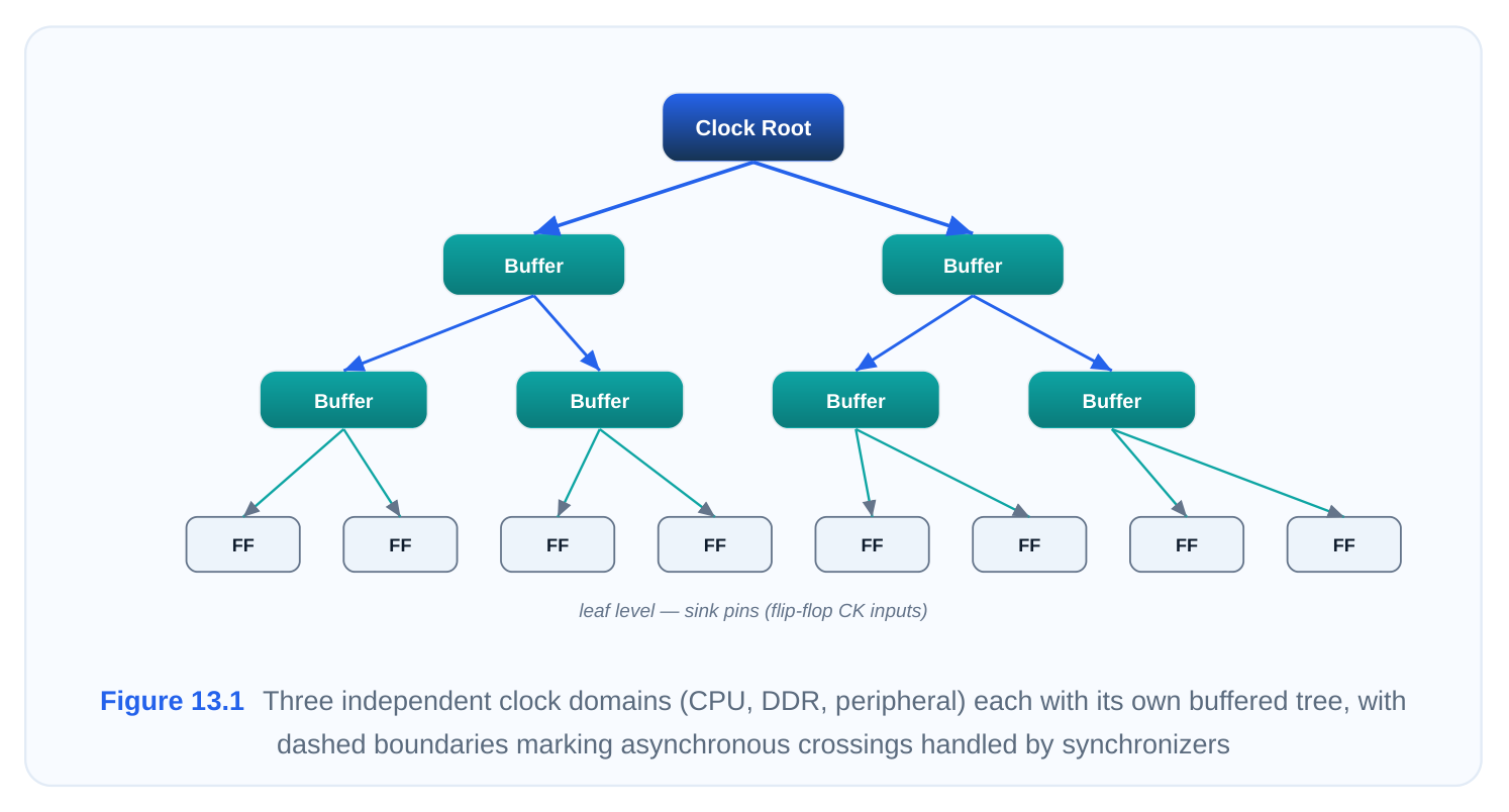
A clock domain is simply the collection of sequential elements that are timed by a common clock. The moment a design contains more than one independent clock, CTS becomes a problem of building sev‐ eral trees that must each meet their own skew and latency targets without interfering with one another. A typical application processor might carry a CPU clock, a DDR controller clock, a USB reference clock, a PCIe clock, and a slow always-on clock for power management — each with different frequency, different criticality, and different physical footprint.
Why isolation matters
The cardinal rule is that asynchronous or unrelated clocks should never be balanced against each other. If the tool tries to equalize insertion delay between a 2 GHz CPU clock and a 32 kHz RTC clock, it will waste enormous buffering effort, burn power, and produce a tree that is fragile to OCV. Worse, balancing unrelated clocks creates artificial timing relationships that have no physical meaning. The
goal is the opposite: keep each domain's tree electrically and logically separate, and only worry about the boundaries where data actually crosses between domains. Isolation is enforced on two fronts. Logically, you tell the tool which clocks are independent so it never tries to share buffers or balance latency across the boundary. Physically, you keep the trees from competing for the same routing tracks and buffer sites in a way that degrades either one.
Stopping the tool from touching specific clocks
When you run CTS, you often want to build only a subset of trees in a given pass, or you want to permanently exclude certain clocks (for example, a clock that is already routed as a special net, or a test clock you will handle separately). The command family for this controls which clocks the synthesizer considers.
# Exclude clocks that should not be synthesized in this pass
set_clock_tree_options -clock {ddr_clk pcie_clk} -target_skew 0.036
# Keep the tool away from a manually handled or test-only clock
prevent_specific_clocks [get_clocks {scan_clk}]
# Confirm which clocks are in scope before launching
report_clock_tree -summary
By marking a clock with prevent_specific_clocks , you guarantee its sinks are not buffered, bal‐ anced, or rerouted by the CTS engine. This is essential for clocks driven from a dedicated structure such as a mesh, an H-tree you built by hand, or a clock that arrives fully formed from a hard macro.
Independent tree synthesis
Each domain is synthesized against its own constraint set: its own target skew, its own maximum insertion delay, its own transition and capacitance limits, and its own buffer/inverter list if the domain needs special cells. A high-speed domain may demand sub-45 ps skew and low-Vt buffers; a slow always-on domain may accept loose skew and insist on high-Vt cells to minimize leakage. Treating them with one global recipe produces a tree that is simultaneously over-engineered for the slow clock and under-engineered for the fast one.
Cross-domain validation
Independent synthesis is necessary but not sufficient. Wherever data flows from one domain into another, the timing must be checked. There are two cases:
| Crossing type | Relationship | CTS implication |
|---|---|---|
| Synchronous (related clocks, e.g. | Defined phase re‐ | Latencies should be balanced across the boundary |
| divided versions) | lationship | so setup/hold solve cleanly |
| Asynchronous (no phase rela‐ | Undefined tionship) | Do not balance; rely on synchronizers and treat the path as false/async |
For synchronous crossings you generally do want some inter-domain balancing so that the launch and capture clocks have a controlled latency difference. For asynchronous crossings you explicitly tell the timer the path is not to be optimized and you depend on metastability-hardened synchronizers. The CTS engineer's job is to know which boundaries are which and to set up the balance groups accord‐ ingly.
Domain-specific constraints
The practical workflow is to define a constraint block per clock — skew target, latency target, usefulskew permissions, NDR (non-default routing) rules, and cell lists — and apply them per clock rather than globally. This keeps each tree honest to its own requirements and prevents the tool from making cross-domain compromises that help no one.
13.2 Generated Clocks with Multiple Parents
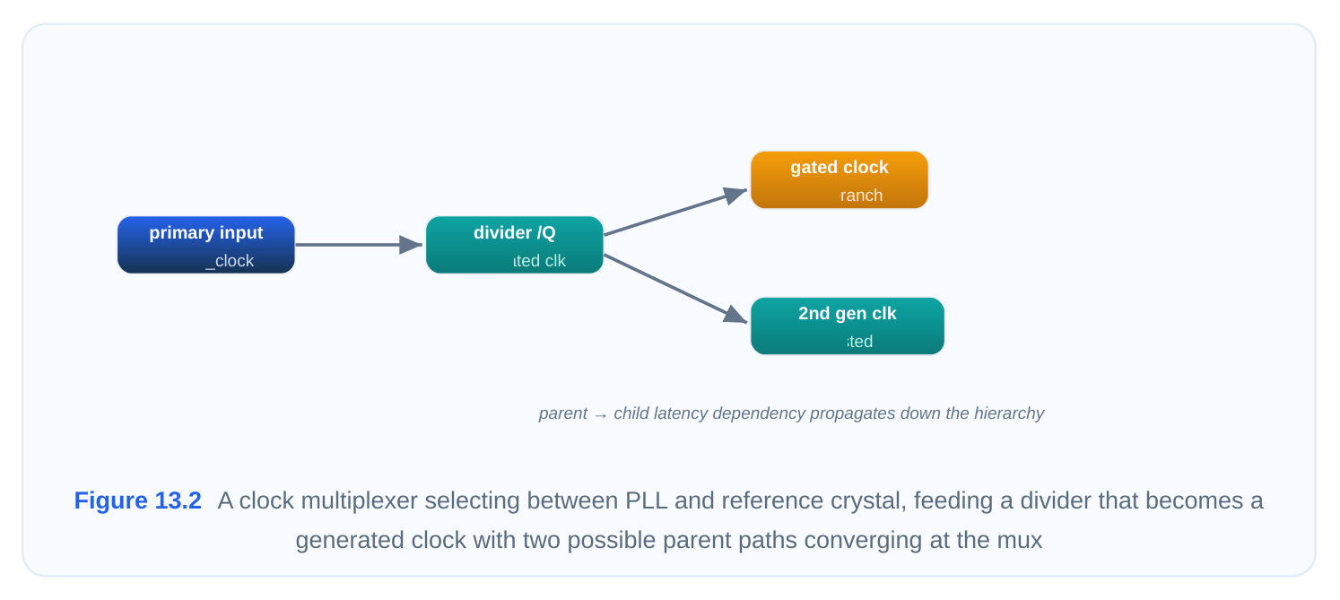
A generated clock is a clock derived from another clock — a divider output, a gated clock, a multiplex‐ er output. Usually a generated clock has a single master. But real designs produce situations where a generated clock can trace back to more than one source: think of a clock mux that selects between a PLL output and a bypass crystal, where the divider downstream is therefore reachable from two par‐ ents.
The multi-parent problem
When a sink can be driven by either of two upstream sources depending on configuration, the tool has to decide what latency to balance to. If it picks one parent's path and ignores the other, the tree will be balanced in one mode and badly skewed in the other. The challenge is to produce a single physical tree that behaves acceptably regardless of which parent is active.
Specifying insertion delay
For multi-parent generated clocks you often need to tell the tool the expected insertion delay at the point where the parents converge, rather than letting it infer a single path. This gives the balancing engine a stable target so both modes see comparable latency from the convergence point onward.
# Define a generated clock at a divider that can be fed by two sources
create_generated_clock -name div_clk -divide_by 2 \
-source [get_pins clk_mux/Z] [get_pins div_reg/Q]
# Tell CTS the convergence point so both parent paths are treated consistently
set_clock_balance_points -consider_for_balancing true \
-balance_point [get_pins clk_mux/Z]
# Provide an insertion-delay expectation downstream of the mux
set_clock_latency 0.250 [get_pins div_reg/CP]
set_clock_balance_points for multi-parent trees
The set_clock_balance_points mechanism lets you nominate explicit nodes where the tool should equalize latency, and exclude nodes where it should not. For a multi-parent clock, you typically declare the mux output as the balance point: everything upstream is left to the individual parent trees, and everything downstream is balanced from that single convergence node. This collapses a two-parent problem into a one-parent problem from the balance point onward.
Cascade clock isolation
When generated clocks cascade — a divider feeds a gate, which feeds another divider — you want to prevent the tool from trying to balance the entire chain end to end as if it were one flat tree. Each stage is isolated so that latency targets are met stage by stage. This keeps the buffering local and avoids a single change rippling through the whole cascade.
Output-port handling
Clocks that leave the die through an output port (for forwarded clocks, source-synchronous interfaces like DDR DQS, or clock outputs to other chips) need their own treatment. You specify the desired latency at the port so the off-chip relationship is correct, and you make sure the tool drives the port with an appropriately sized buffer for the board load rather than an internal-only buffer.
13.3 Post-CTS Optimization
Building the tree is only half the story. Once clocks are real — with real buffers, real routing, and real propagated latency — the timing picture changes completely. Setup and hold must be re-solved against propagated clocks, and the inserted buffers may have created new congestion or power hot‐ spots. Post-CTS optimization is the cleanup and improvement pass that follows synthesis.
The clock_opt command
clock_opt is the umbrella command that, in a single invocation, builds the clock tree and then runs optimization on the result. In modern flows it encapsulates several stages: initial tree synthesis, postCTS setup optimization, hold fixing, and routing preparation. You can run it end to end or break it into phases for finer control.
# Full clock build plus optimization in one shot
clock_opt
# Phased control: synthesize first, then optimize timing only
clock_opt -only_cts -no_clock_route
report_clock_tree -summary
# Run the optimization phase separately after inspecting the raw tree
clock_opt -from final_opto
Timing improvement
After CTS, the timer switches from ideal to propagated clocks. Setup paths that looked fine with an ideal zero-skew clock now carry real insertion delay and real skew, and some will fail. The optimizer fixes these by resizing logic, restructuring, inserting buffers on data paths, and — critically — by exploiting useful skew, deliberately shifting clock arrival at selected registers to borrow time across
stage boundaries. Hold violations, which CTS itself can introduce because added latency changes relative arrival times, are repaired by padding the fast paths with delay cells.
Power and area optimization
The same pass attacks dynamic and leakage power. Clock buffers are among the most power-hungry cells in the design because they switch every cycle and drive large loads, so the optimizer will downsize buffers where slack allows, swap cells to higher-Vt variants on non-critical branches, and remove redundant buffering. Area recovery folds in here too: any cell that can shrink without breaking timing is shrunk.
| Optimization objective | Typical levers | Risk if over-applied |
|---|---|---|
| Setup timing | Useful skew, resizing, buffer insertion on data | Hold violations, more clock power |
| Hold timing | Delay-cell padding on fast paths | Area and leakage growth |
| Dynamic power | Buffer downsizing, gating, load balancing | Transition/skew degradation |
| Leakage power | High-Vt cell swaps on non-critical branches | Slower paths, setup risk |
Legalization and routing preparation
Every cell the optimizer adds or resizes must end up on a legal placement site without overlaps, and the clock nets must be prepared for detailed routing — often with non-default rules (wider wires, extra spacing, shielding) so the clock is resistant to crosstalk and EM. Legalization and route prep at the end of clock_opt hand a clean, routable database to the next stage.
13.4 Multisource Clock Trees
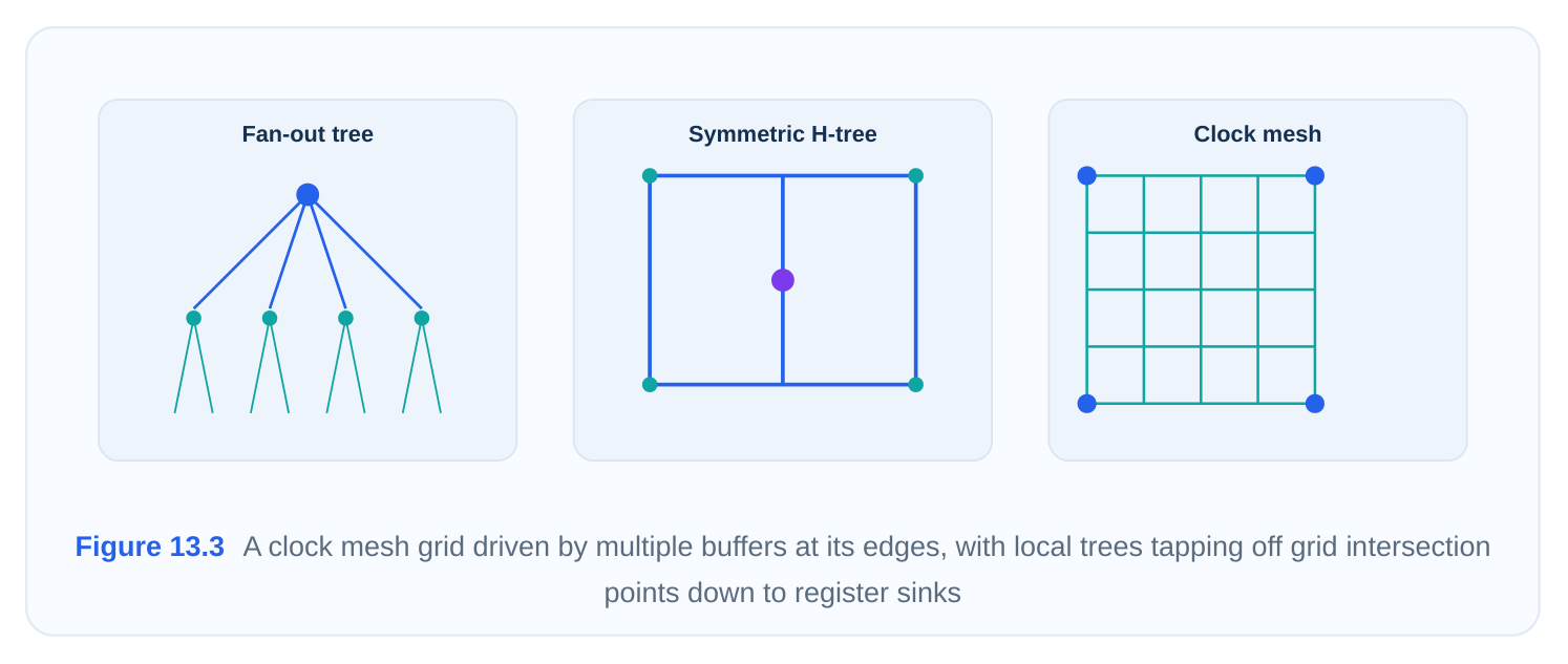
A multisource clock tree (sometimes called a clock mesh or a multi-tap tree depending on the imple‐ mentation) is a strategy where a single clock is distributed through multiple driving points that all converge on a low-impedance backbone, rather than through one strictly hierarchical H-tree. The classic example is a clock mesh: a grid of wire driven by many buffers in parallel, with sinks tapped off the nearest grid point.
Why use multiple sources
The motivation is skew robustness. In a conventional tree, skew accumulates along the longest branch and is highly sensitive to on-chip variation, because the launch and capture clocks travel through different buffer chains. A mesh or multi-driven backbone shorts out those differences: because the grid is electrically tied together, local variation between neighboring taps is heavily suppressed. The price is power — driving a big mesh costs a lot of dynamic energy — so this technique is reserved for the most skew-critical clocks, typically the top-level CPU clock.
Integrated tap assignment
In a multisource flow the tool must decide which mesh node (tap point) each sink connects to and then build a short local tree from that tap to the registers. Good tap assignment minimizes the local-tree depth so that almost all of the latency-equalizing work is done by the mesh itself, leaving only short, well-matched local branches.
Multiple master sources and shared portions
Some clocks have genuinely multiple master sources — for instance, a redundant clock scheme or a clock that can be sourced from two PLLs for reliability. Here the trees from each master share the downstream backbone but diverge upstream. The flow has to recognize the shared portion and build it once, while keeping the per-master upstream segments independent.
# Declare a multisource (mesh-style) distribution for the critical clock
set_clock_tree_options -clock cpu_clk \
-tree_type multisource
# Define the mesh region and the driver set that feed it
create_clock_mesh -clock cpu_clk \
-region {100 100 900 900} \
-drivers [get_cells {mesh_drv_*}]
# Constrain how local trees connect to the mesh taps
set_clock_balance_points -clock cpu_clk \
-tap_selection nearest
Tap-point selection and master-clock hierarchy
Tap selection balances two goals: nearest-tap for short local trees, versus load-balanced taps so no single mesh node is overloaded. The master-clock hierarchy describes how the multisource clock relates to its generated children — a divided version of the meshed clock, for example, should inherit
the mesh as its parent and only build a local divider-output tree, not a second independent backbone. Getting this hierarchy right ensures the divided clock enjoys the same skew robustness as its master.
13.5 Clock Gating Integration
Clock gating is the single most effective dynamic-power technique in digital design: an integrated clock gating (ICG) cell shuts off the clock to a block of registers when their enable is inactive, eliminating switching power in both the registers and the downstream clock branch. But gates sit inside the clock tree, which means CTS must treat them as first-class citizens, not obstacles.
Gated clock tree synthesis
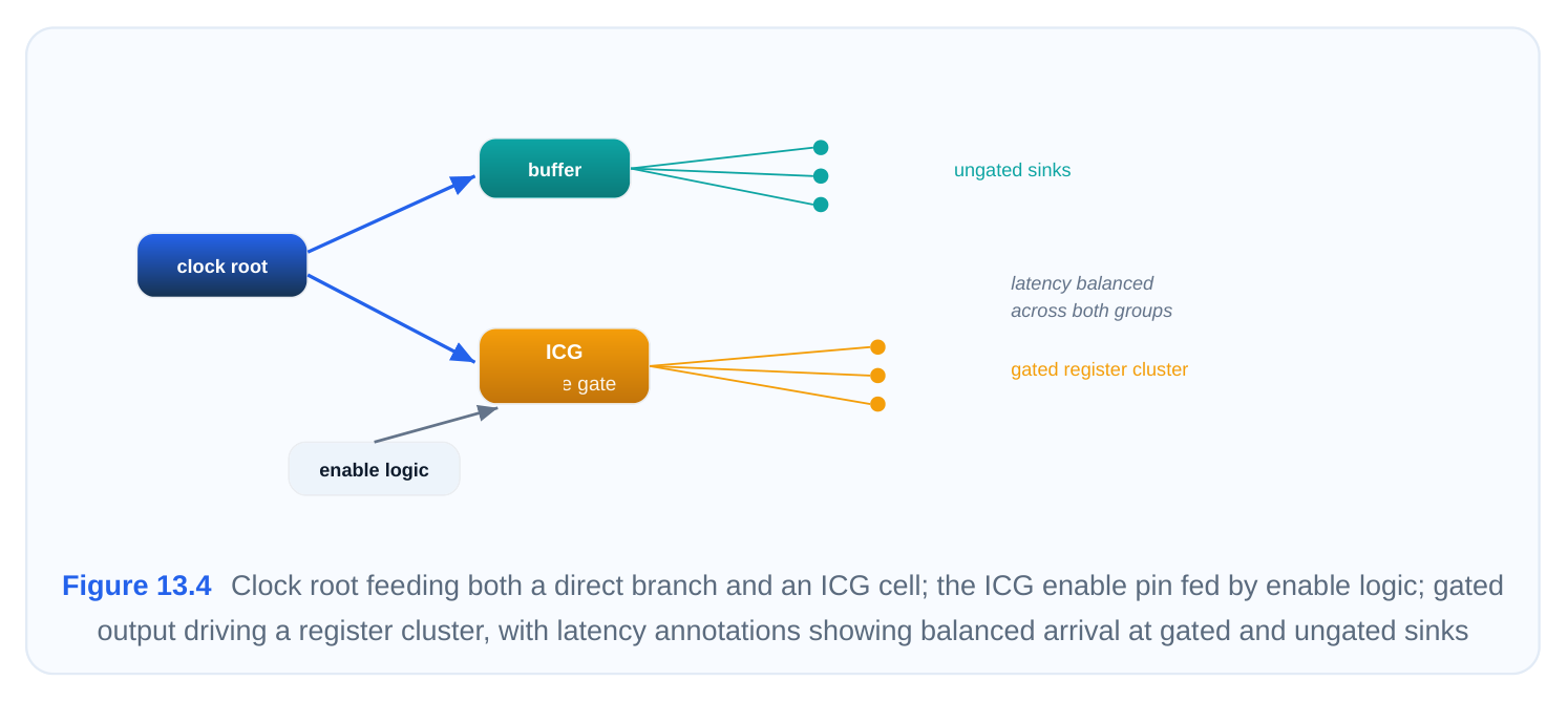
An ICG cell is a buffer-with-a-switch from the tree's perspective: the clock enters its CK pin and leaves its gated-clock output (often ECK or GCLK). CTS must balance through the gate — the latency from the root to a register downstream of a gate must match the latency to an ungated register so that skew across the domain is controlled. The tool models the ICG as a node in the tree and continues balancing past it.
Enable-pin handling and enable timing
The enable input of an ICG is itself a timing endpoint. The enable must be stable before the relevant clock edge or the gate can glitch or chop a pulse. Latch-based ICG cells exist precisely to absorb enable timing by latching the enable on the opposite phase, but the setup/hold on the enable pin relative to the clock still has to be met. After CTS shifts the clock latency, enable paths must be retimed because the clock at the ICG moved.
# Tell CTS to balance through clock gating cells
set_clock_tree_options -clock core_clk \
-gate_balancing true
# Constrain the enable arrival relative to the gating cell's clock
set_clock_gating_check -setup 0.080 -hold 0.030 \
[get_cells icg_core_*]
# Keep gating cells from being relocated far from their register cluster
set_clock_tree_exceptions -balance_skew_group gated_grp \
-through [get_pins icg_core_*/GCLK]
Gating-logic impact and placement
Where the gate physically sits matters. Placing the ICG close to the register cluster it serves shortens the gated branch and maximizes the power saving (the disabled branch is large), but it can lengthen the enable path. The tool, with guidance, places gates to balance these forces. Gating also affects skew: because the gated branch only toggles sometimes, its loading and the optimization around it differ from always-on branches.
Optimization with gating
During clock_opt , the engine can clone gates to split heavily loaded enables, merge redundant gates, resize them, and adjust where they sit in the hierarchy. The optimizer also accounts for the fact that gated power only counts when the gate is enabled, so it weighs activity factors when deciding how aggressively to optimize a particular branch. Done well, gating integration delivers large dynamicpower wins without sacrificing the skew budget.
13.6 High-Speed Clock Distribution
When a clock runs at multiple gigahertz, the period shrinks to hundreds of picoseconds, and skew that would be invisible at 100 MHz becomes a dominant fraction of the cycle. High-speed distribution is the discipline of holding skew to extremely tight bounds — often under 45 ps — while keeping transition times sharp and jitter low.
The sub-45 ps requirement
At a 4 GHz clock the period is 225 ps. If skew alone eats 45 ps, that is 18% of the budget gone before any logic delay or setup margin is considered. Achieving sub-45 ps skew demands symmetric struc‐ tures (balanced H-trees or meshes), matched buffer chains, controlled wire lengths, and tight transition control so that every sink sees a near-identical edge. Variation must be suppressed, which is why high-speed clocks often use the mesh approach from 13.4.
High-effort timing mode and constraint selection
Tools expose effort levels; high-speed clocks justify the highest effort, accepting longer runtime for tighter results. Constraint selection is deliberate: aggressive target skew, tight maximum transition (a slow edge increases delay sensitivity to variation and worsens duty-cycle distortion), and conservative capacitance limits.
# Push the tool to maximum effort for the high-speed clock
set_clock_tree_options -clock hs_clk \
-target_skew 0.027 \
-max_transition 0.054 \
-optimization_effort high
# Apply non-default routing: wider, shielded wires for the high-speed net
set_clock_routing_rules -clock hs_clk \
-rule double_width_double_space -shield true
# Restrict to fast, low-Vt buffers for the speed-critical branches
set_clock_tree_references -clock hs_clk \
-references {BUFFD8LVT BUFFD12LVT INVD8LVT}
Buffer technology and layout preparation
High-speed trees lean on low-threshold (low-Vt) buffers for speed, accepting their higher leakage. Wire engineering matters as much as cell choice: non-default routing with wider metal lowers resistance and EM risk, and shielding (grounded neighbors) suppresses crosstalk-induced jitter. Layout prepara‐ tion reserves routing tracks and buffer sites along the intended distribution path early, so the highspeed structure is not forced into a congested region after the fact. Many flows pre-place the top-level buffers and the mesh drivers before general placement to lock in symmetry.
| Parameter | Low-speed clock | High-speed clock (>2 GHz) |
|---|---|---|
| Skew target | 100–180 ps acceptable | < 45 ps, often < 27 ps |
| Buffer Vt | High-Vt (low leakage) | Low-Vt (fast) |
| Routing | Default rules | NDR: wide + shielded |
| Structure | Standard tree | Mesh or symmetric H-tree |
| Effort | Medium | High |
| Power priority | High | Secondary to timing |
13.7 Power-Constrained Designs
In mobile, IoT, and many edge SoCs, the clock network is the largest single consumer of dynamic power — frequently 28–46% of the chip total — because it toggles every cycle and drives huge fanout. When a project hands you a power budget, the clock tree is where you must spend it wisely.
Clock power budgets
A power-constrained CTS run starts with an explicit ceiling: a maximum allowed clock dynamic power, sometimes broken down per domain. You then steer the tool to honor it by trading away the things you do not need — loose skew where the design tolerates it, fewer and smaller buffers, and aggressive gating. The discipline is to spend tight skew only on the clocks that need it and let everything else run lean.
Dynamic versus leakage optimization
The two components of clock power pull in different directions:
- Dynamic power scales with switched capacitance and frequency. You reduce it by minimizing buffer count, downsizing buffers, shortening wires, and — most powerfully — gating so branches stop toggling when idle.
- Leakage power is the static drain of every transistor, dominated by low-Vt cells. You reduce it by using high-Vt buffers wherever the timing margin allows, since clock buffers are numerous and their leakage adds up.
# Set a clock power ceiling and bias optimization toward powerset_clock_tree_options -clock io_clk \-power_effort high \-max_clock_power 8.0# Prefer high-Vt buffers to cut leakage on non-critical clocksset_clock_tree_references -clock io_clk \-references {BUFFD2HVT BUFFD4HVT}# Maximize gating opportunities during optimizationclock_opt -power_optimization true -insert_clock_gating true
Technology-node considerations
The node changes the balance. At older nodes (28 nm and above), dynamic power dominates and leakage is modest, so the priority is buffer reduction and gating. At advanced FinFET nodes leakage is better controlled by the device but density is far higher, so dynamic power per area climbs and clock distribution becomes even more dominant — pushing teams toward meshes only where essential and aggressive gating everywhere else. Multi-Vt libraries give you the knob to trade speed for leakage branch by branch.
Power-aware placement and area trade-offs
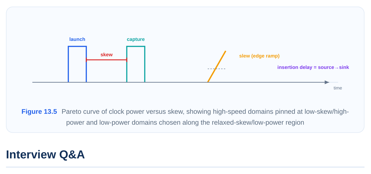
Power-aware CTS places buffers to minimize total wirelength, because wire capacitance is switched capacitance — shorter clock wires directly mean lower dynamic power. It clusters sinks so a single buffer drives a tight group rather than reaching across the die. The fundamental trade-off is skew versus power: a tighter skew target generally requires more and bigger buffers, which costs power and area; relaxing skew on tolerant domains frees both. The art of power-constrained CTS is knowing exactly how much skew each domain can give up.
CTS? Asynchronous clocks have no defined phase relationship, so equalizing their insertion delays creates a timing relationship that is physically meaningless. It wastes buffering and power, makes the trees more sensitive to on-chip variation, and provides no benefit because data crossing between the domains must go through synchronizers regardless. You isolate the domains and treat the crossings as asynchronous false paths, relying on metastability-hardened synchronizers instead.
ents? It lets you nominate explicit nodes — typically the convergence point such as a clock-mux output — where the tool should equalize latency, and exclude nodes where it should not. For a multiparent clock this collapses the problem: everything upstream of the balance point is handled by the individual parent trees, and everything downstream is balanced from that single node, giving consistent latency regardless of which parent is active.
ideal clocks with propagated clocks carrying real insertion delay and real skew. Adding latency to one branch changes the relative arrival of launch and capture edges, and where the capture clock now arrives earlier relative to the launch clock, fast data paths can violate hold. The post-CTS optimization pass repairs these by inserting delay (buffer/delay cells) on the offending fast paths.
You choose a mesh for the most skew-critical, highest-frequency clock (usually the top-level CPU
clock) because the electrically tied grid suppresses local variation between neighboring taps far better than a hierarchical tree, yielding very low and very robust skew. The cost is power: driving a large mesh consumes substantial dynamic energy, so it is reserved for clocks where skew robustness justifies that expense.
tegrated clock gating cell sits in the clock path, so the tool must balance latency through it — the rootto-register latency for gated registers must match that of ungated registers to keep domain skew controlled. The enable pin becomes a timing endpoint with its own setup/hold (clock-gating check) that must be met relative to the gate's clock, and because CTS shifts clock latency, enable paths are retimed after the tree is built. The optimizer can clone, merge, resize, and reposition gates while respecting these constraints.
Key Takeaways
- Multiple clock domains are synthesized independently with per-domain constraints; isolate unre‐ lated clocks and balance only synchronous crossings, leaving asynchronous ones to synchron‐ izers.
- Multi-parent generated clocks are tamed with
set_clock_balance_pointsat the convergence node, plus explicit insertion-delay specs and stage-by-stage isolation of cascaded clocks. clock_optbuilds the tree and then re-solves setup with useful skew, fixes the hold violations CTS itself introduces, recovers power and area, and prepares nets for routing.- Multisource trees and meshes trade dynamic power for outstanding skew robustness and are reserved for the most timing-critical, high-frequency clocks.
- Clock gating is the top dynamic-power lever, but gates must be balanced through, their enables timed, and their placement chosen to maximize savings without breaking skew.
- Power-constrained CTS spends tight skew only where required, uses high-Vt buffers and gating to cut leakage and dynamic power, and treats shorter clock wirelength as direct power savings — with skew-versus-power as the central trade-off.
Comments
Leave a Reply