 ChipBuddy
← Home
ChipBuddy
← Home
The MSV Top-Down Hierarchical Flow
When a System-on-Chip grows past a few million instances, the comfortable idea of laying out the whole thing as one giant flat database stops being practical. Placement, routing, and timing closure all scale super-linearly with instance count, machine memory becomes the limiting resource long before the algorithms do, and a single optimization run can take days only to be invalidated by one late RTL change. Add multi-supply-voltage (MSV) low-power techniques on top of that — voltage areas, level shifters, isolation, power switches — and a flat approach becomes nearly impossible to converge or even debug. The industry's answer is hierarchical implementation: cut the chip into manageable blocks, build each one against a contract, and stitch them back together. This chapter focuses on the top-down hierarchical flow, where the major decisions are made at the full-chip level first and then propagated downward. We will walk the three stages, see how power intent is split across the hierarchy, examine the awkward problem of routing signals through blocks that sit at different voltages, and weigh the trade-offs that make this flow powerful but unforgiving.
Why Hierarchy, and Why Top-Down
Hierarchical implementation breaks a design into partitions (also called blocks or physical blocks). Each partition is implemented as a self-contained layout with its own placement, clock tree, routing,
and abstract (a lightweight model of its boundary and timing used by the parent). The top level then treats each finished block as a black box with a known shape, known pin locations, and known timing characteristics. The defining property of top-down is the direction of decision flow. The full-chip context is established first: the die size, the location and shape of every block, the global power grid, and where each voltage area lives. From that full-chip picture, the team budgets timing, area, and power down to each block and pushes down the constraints that the block must honor at its boundary. Only then does block-level work begin. Contrast this with a bottom-up flow, where blocks are hardened in isolation first and the top level must accept whatever footprints and timing they happen to produce.
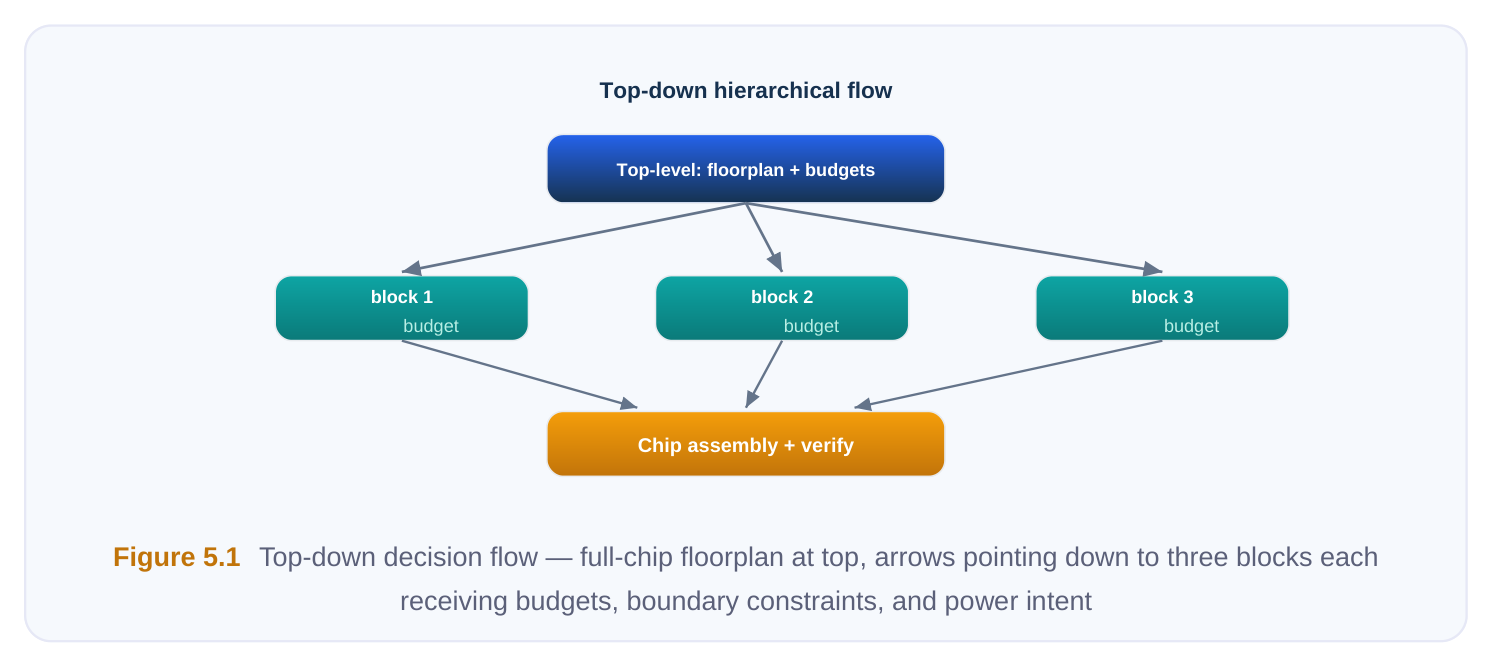
The top-down approach trades early commitment for early control. Because the full-chip floorplan and power network are decided up front, the team can reason about chip-level concurrency, package and bump planning, and the global power delivery network before sinking effort into block internals.
The Three Stages
A top-down MSV flow is best understood as three sequential stages, each with a distinct owner and deliverable.
| Stage | Primary inputs | Key activities | Deliverables to next stage |
|---|---|---|---|
| 1. Top-level | Full netlist, die/ | Chip floorplan, partition shaping, | Block shapes, pin |
| implementation | package constraints, top power intent | top power grid, voltage-area definition, timing/area/power budgeting, constraint and intent push-down | locations, boundary constraints, per-block budgets, block-level power intent |
| 2. Block-level | Block netlist, | Place, CTS, route, insert low- | Hardened block layout + |
| implementation | pushed-down constraints, block | power cells (level shifters, ISO, switches), close block timing/ power intent | timing/physical/power abstract power, generate abstract |
| 3. Chip assembly | Top floorplan + all hardened block | Place blocks, connect power, route top-level interconnect and abstracts | Signed-off full-chip database feedthroughs, verify interfaces and |
cross-block power
STAGE 1 — TOP-LEVEL IMPLEMENTATION
This is where the chip's skeleton is defined. The engineer creates the full-chip floorplan, decides how many partitions there will be, and gives each one a shape — usually rectilinear, sometimes a simple rectangle — sized to hold its logic with reasonable utilization. The top-level power network is planned here: the main rings, the global straps, and the trunks that will feed each voltage area. Because this is an MSV design, the engineer also defines the voltage areas — the physical regions that will operate at a particular supply — and maps each block (or group of blocks) onto the appropriate area. Two push-down activities make or break the stage. First, budgeting: the top-level timing, area, and power targets are divided among the blocks. A block receives a slice of the total timing path (its boundary timing budget), a power ceiling consistent with the MSV plan, and an area/utilization target consistent with its allotted shape. Second, constraint and intent push-down: the interface (boundary) constraints — input delays, output delays, and the timing context seen at each block port — are derived from the top-level context and handed to the block, together with the block's slice of the power intent.
# Stage 1 sketch: define a voltage area and shape a partition
create_voltage_area  VA_LOW  -coordinate {1200 800 2400 1900} -domain PD_CORE_LOW
create_partition     blk_dsp -boundary {200 200 1100 1100}
create_partition     blk_io  -boundary {200 1200 1100 2000}
assign_block_to_voltage_area blk_dsp VA_LOW
# Budget and push interface constraints + power intent down to a block
derive_boundary_timing  -partition blk_dsp -from_top_constraints top.sdc
set_block_budget        blk_dsp -power 18mW -area_util 0.72
push_constraints        blk_dsp -timing blk_dsp.sdc -power_intent blk_dsp.upf
The quality of Stage 1 is everything. Budgets that are pushed down become hard targets for every block team; if they are wrong, the error is not discovered until assembly, when it is most expensive to fix.
STAGE 2 — BLOCK-LEVEL IMPLEMENTATION
Each block is now implemented independently, in its own session, by its own engineer or team. The block receives its shape, its pin constraints, its boundary timing ( .sdc ), and its power intent ( .upf or .cpf ). From there it runs a complete physical flow: placement, clock tree synthesis, routing, and timing/power closure — all confined to the block boundary and judged against the pushed-down budget. For MSV, this is where most low-power cells physically land. The block inserts and legalizes its own level shifters on signals crossing between its internal voltage and a neighboring one, its isolation cells on outputs of switchable domains, and, if it contains a switchable region, its power switches (header/footer arrays) and the local switched-supply distribution. The retention strategy for any stateretaining registers inside the block is realized here too.
# Stage 2 sketch: implement a block against its pushed-down contract
read_netlist     blk_dsp.v
read_constraints blk_dsp.sdc
load_power_intent blk_dsp.upf      ;# IEEE 1801 (UPF); CPF equally valid
place_design
insert_level_shifters  -on_crossings {VA_LOW <-> VA_HIGH}
insert_isolation_cells -domain PD_DSP_SW -clamp 0
synthesize_power_switch -domain PD_DSP_SW -style header
clock_tree_synthesis
route_design
verify_block_budget blk_dsp        ;# confirm timing/area/power within budget
write_abstract      blk_dsp -physical -timing -power
The block's final product is a layout plus an abstract. The abstract captures only what the parent needs: the boundary outline, pin positions and layers, a timing model, blockage information, and a power model (which rails the block expects and how it draws current). The parent never re-opens the block's internals; it trusts the abstract.
STAGE 3 — CHIP ASSEMBLY
Assembly brings the hardened blocks back to the top level and integrates them into a single signed-off database. The blocks are placed into their reserved locations, the top-level power network is connected to each block's rails (each block must mate cleanly to the right voltage area's straps), and the top-level interconnect — including any feedthroughs — is routed. Verification at assembly is where hierarchical and MSV concerns meet. The engineer checks that boundary timing actually closes when blocks see each other's real arrival times (not just the pushed-
down estimates), and runs cross-block low-power verification: every domain crossing has the correct level shifter, every switchable domain's outputs are isolated, the always-on routing reaches every switch controller, and no block draws from a rail the assembly did not connect.
# Stage 3 sketch: assemble blocks and verify the chip
read_floorplan      top.fp
place_block         blk_dsp -at {200 200}
place_block         blk_io  -at {200 1200}
connect_block_power blk_dsp -to VA_LOW
connect_block_power blk_io  -to VA_HIGH
route_top_level
verify_interfaces   -timing -power
verify_power_intent -hierarchical    ;# level shifters, isolation, always-on
integrity
How Power Intent Partitions Across the Hierarchy
A single MSV intent description for the whole chip would be unwieldy and would defeat the purpose of hierarchy. Instead, the intent is split: a top-level intent file describes the chip-wide structure, and each block carries a scoped intent file describing its own internals. The two must agree at the boundary. The top-level intent owns the things only the parent can know: the full set of supply nets, the power domains and which blocks belong to them, the voltage-area-to-domain mapping, and the connection rules at block boundaries — for example, that a particular block port is a domain crossing requiring a level shifter, or that a block's outputs feed an always-on consumer and must be isolated when the block powers down. The per-block intent owns the block's internal domains, its switchable regions, the supply set the block sees at its ports, and the rules governing crossings inside the block. Intent
Owns Examples
| Top- | Chip-wide supplies, domain-to-block | Global VDD/VDD_LOW/VSS nets, "block DSP is in |
|---|---|---|
| level | mapping, voltage areas, boundary crossing rules | PD_CORE_LOW", boundary level-shifter and isolation rules |
| Per- | Internal domains, switchable regions, | Block-internal switched domain, in-block level shifters, |
| block | port supply context, internal crossing | retention list, header switch strategy |
rules The discipline that ties the two layers together is the boundary contract: the supply context a block assumes at its ports must be exactly what the top level connects there. If the block was implemented assuming its data_out port drives the low-voltage area but assembly wires it to a high-voltage consumer, you get a missing or wrong-direction level shifter — a classic hierarchical MSV bug caught only by full-chip power verification. Many teams formalize this by generating each block's intent from the top intent during Stage 1, so the two cannot drift apart.
Interface and Feedthrough Handling Between Different-Voltage Blocks
Two physical realities make MSV interfaces tricky. First, any signal crossing a voltage boundary needs conditioning — a level shifter to translate logic levels, and isolation if either side can be powered down. The flow must decide which side owns each shifter. Common practice places the level shifter inside the destination block (or in a thin interface region), and the boundary contract records this so the same crossing is not double-shifted or left unshifted. Second, feedthroughs. A wire from block A to block C may have to cross block B because B sits geographically between them. Since the parent treats B as a black box, that wire cannot simply be routed over B's hardened layout without permission — B has internal routing and may have routing blockages. The clean solution is to plan dedicated feedthrough paths (sometimes called routing channels or feedthrough pins/buffers) inside B during Stage 1, reserve those tracks in B's abstract, and let assembly route through them. When the feedthrough passes through a block at a different voltage, the signal must remain in a consistent supply context the whole way; if B is a low-voltage island and the feedthrough net is a high-voltage signal, the channel must carry the correct rail or the net must be buffered with appropriately powered cells.
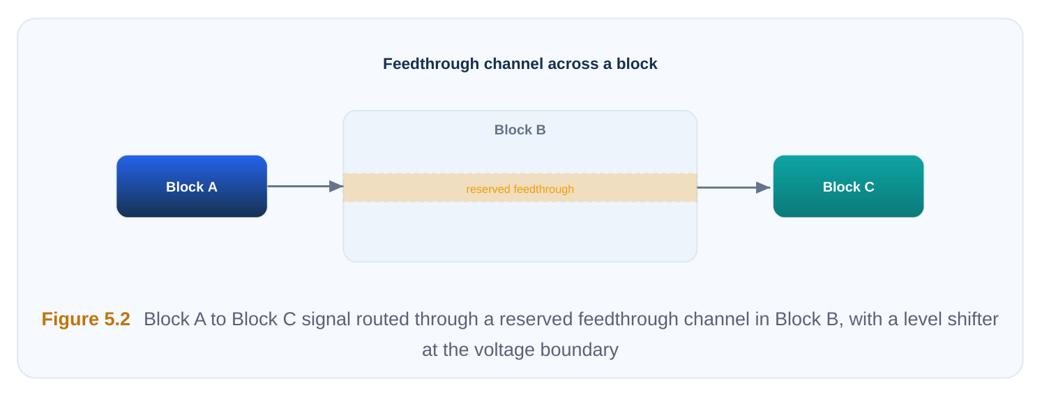
Planning feedthroughs up front is the top-down win here: because the parent owns the floorplan first, it can carve out these channels before any block is hardened. Discovering the need for a feedthrough after blocks are closed is a costly re-spin of an already-finished block.
Pros and Cons of Top-Down
The top-down flow's great virtue is early full-chip control. Floorplan, power network, voltage areas, and the global timing picture are settled before block effort is committed, which is exactly what you want when power delivery and MSV partitioning are first-class concerns. Blocks can then be built concurrently by separate teams, each turning quickly in a small database, and a localized RTL change ideally re-hardens only its block rather than the whole chip. The matching risk is that everything rides on the budgets. The push-down step makes assumptions — about boundary arrival times, about how much power each block may burn, about utilization — and if those assumptions are wrong, blocks close cleanly against bad targets and the failure surfaces only
at assembly. Re-budgeting then forces blocks to be re-implemented, the most expensive kind of iteration. The abstraction that gives the flow its speed also hides cross-block interactions: optimistic boundary models can mask paths that only fail when real neighbors are present. And the up-front commitment to a floorplan means a late architectural change can invalidate partitioning that was expensive to create.
| Aspect | Top-down strength | Top-down risk |
|---|---|---|
| Control | Full-chip floorplan/power/MSV decided | Locks in floorplan before block reality is known |
early
| Schedule | Concurrent block work; fast local turns | Bad budgets force costly block re-spins |
|---|---|---|
| Interfaces | Feedthroughs and crossings planned up | Optimistic boundary models hide real failures |
front
| Power | Clean top + per-block split | Boundary-contract drift creates MSV bugs at |
|---|---|---|
| intent | assembly |
In practice, teams hedge with conservative initial budgets, early boundary-timing sanity checks before blocks fully close, and iterative re-budgeting in the first couple of full-chip assembly trials — accepting some rework early to avoid catastrophic rework late.
Interview Q&A
bottom-up? Top-down means the major decisions — floorplan, power network, voltage areas, and the budgets and constraints for each block — are made at the full-chip level first and then pushed down to the blocks, which are implemented to honor that context. Bottom-up hardens blocks in isolation first and forces the top level to accept their resulting shapes and timing. Top-down gives early full-chip control at the cost of committing to budgets that may prove wrong; bottom-up gives realistic block data first but less global control early on.
bug? The intent is split into a top-level file (chip-wide supplies, domain-to-block mapping, voltage areas, and boundary crossing rules) and a per-block file scoped to each block's internal domains, switchable regions, and port supply context. The most common bug is boundary-contract drift: the supply context a block assumed at its ports does not match what assembly actually connects, producing a missing, redundant, or wrong-direction level shifter or isolation cell. Generating block intent from the top intent prevents this.
already hardened. How do you handle it? You route it through a pre-planned feedthrough channel reserved inside block B during top-level floorplanning, with those tracks recorded in B's abstract. You do not route arbitrarily over a hardened block. If B is at a different voltage than the feedthrough net, the
channel must carry the correct rail (or use appropriately powered buffers) so the signal stays in a consistent supply context, and a level shifter is placed at the actual voltage boundary.
Because timing/area/power targets are pushed down before block reality is known, blocks can close against wrong targets, with the failure only appearing at chip assembly and forcing expensive reimplementation. Mitigation: start with conservative budgets, run early boundary-timing checks before blocks fully close, build abstracts and do a trial assembly early, and plan for one or two re-budgeting iterations rather than assuming the first push-down is correct.
Key Takeaways
- Hierarchical implementation splits a too-large design into blocks built against contracts; top-down means full-chip decisions (floorplan, power grid, voltage areas, budgets, constraints, intent) flow downward to the blocks.
- The flow has three stages: top-level implementation (floorplan, power network, voltage areas, budgeting, push-down), block-level implementation (independent closure plus insertion of the block's own level shifters, isolation, and switches), and chip assembly (place blocks, connect power, route feedthroughs, verify interfaces and cross-block power).
- Power intent partitions into a top-level layer (chip-wide structure and boundary rules) and per- block layers (internal domains and crossings); the boundary contract must be exact, and generating block intent from top intent prevents drift.
- Interfaces and feedthroughs between different-voltage blocks need level shifters/isolation at crossings and pre-planned routing channels through intervening hardened blocks, all reserved up front while the parent still owns the floorplan.
- Top-down buys early full-chip control and concurrency but stakes everything on correct budgets; conservative targets, early boundary checks, and planned re-budgeting are the standard defenses against late, expensive rework.
Comments
Leave a Reply