 ChipBuddy
← Home
ChipBuddy
← Home
Introduction to Clock Tree Synthesis
1.1 What is Clock Tree Synthesis?
Every synchronous digital chip lives and dies by one signal: the clock. Flip-flops, latches, memory macros, and clocked I/O cells all sample data on a clock edge, and they all assume that the edge arrives "at the same time" everywhere. In reality, a single clock source — typically a PLL output or a pin at the boundary of a block — has to fan out to tens of thousands or even millions of clocked endpoints scattered across the floorplan. Clock Tree Synthesis (CTS) is the physical-design step that builds the network of buffers, inverters, and wires that carries the clock from that single origin to every one of those endpoints, while keeping the arrival times tightly controlled. Before CTS runs, the clock is usually represented as an ideal net. The placement tool and the early timing engine pretend the clock reaches every flip-flop instantaneously, with zero delay and zero transition time. That assumption is convenient for getting the data path placed and roughly timed, but it is physically impossible. A net driving a million loads with no buffering would have astronomical RC delay and a transition time measured in nanoseconds. CTS replaces this fiction with a real, buildable structure: a propagated clock with genuine delays, genuine slews, and genuine differences in arrival time from one endpoint to another.
The buffer-tree structure
The defining shape of a clock distribution network is a tree. Think of the clock source as the root. From the root, the signal passes through a first level of buffers; each of those drives a second level; and so on, level after level, until the final stage of buffers (often called the sink drivers or leaf buffers) connects to the actual flip-flop clock pins, which are the leaves or sinks of the tree.
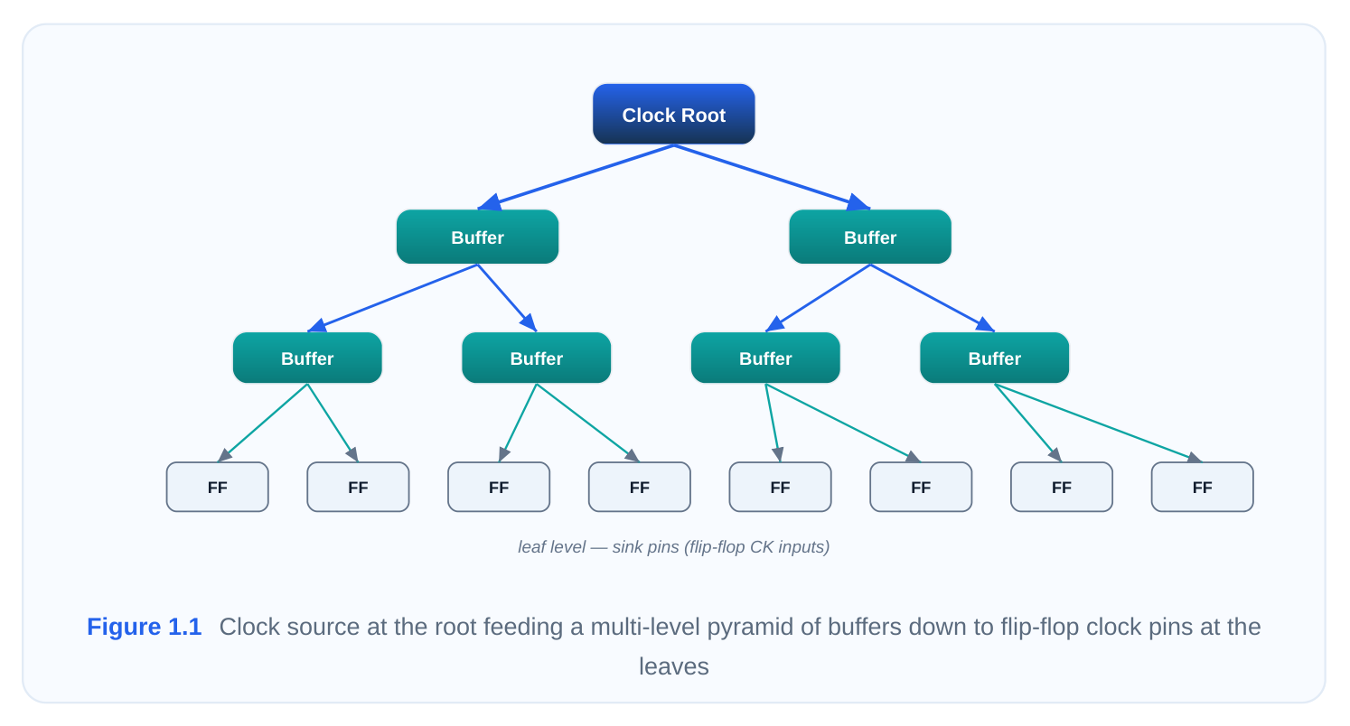
This hierarchical, branching arrangement is not arbitrary. It exists because of a hard electrical constraint: any single gate can only drive a limited capacitive load before its output transition becomes unacceptably slow. By splitting the fanout across many levels, each buffer sees a manageable load, the transition stays sharp, and the total delay stays bounded. A flat structure cannot achieve this; a balanced tree can. We can summarize the vocabulary of the tree like this:
| Term | Meaning |
|---|---|
| Root / clock source | The origin of the clock (PLL output, clock port, or a defined pin) |
| Clock tree cells | Buffers and inverters inserted by CTS to drive intermediate loads |
| Sink / leaf | A clocked endpoint — flip-flop CK pin, latch enable, macro clock pin |
| Branch | A path from the root toward a subset of sinks |
| Level / stage | A rank of buffers at the same depth from the root |
| Clock net segment | The metal wire connecting one driver to its loads |
The purpose of CTS, stated plainly, is to distribute the clock to all endpoints in a controlled, balanced, and electrically clean way — so that the timing the rest of the flow depends on is real
rather than assumed. Everything else CTS does (balancing skew, fixing slew, managing power) is in service of that one goal.
1.2 Why CTS Matters
It is tempting to think of CTS as "just buffer insertion." In practice it is one of the highest-leverage steps in the entire physical-design flow, because it simultaneously determines whether the chip can close timing, how much power it burns, and how much area the clock infrastructure consumes.
Impact on timing closure
Setup and hold checks are written in terms of clock arrival times at the launching and capturing flipflops. When the clock is ideal, those arrival times are all equal, so the timing reports before CTS are optimistic and incomplete. The moment the clock becomes propagated, real differences in arrival time appear, and these differences directly add to or subtract from every setup and hold margin in the design. A poorly built tree can wreck timing that looked perfectly fine pre-CTS. If the capture flop's clock arrives much later than the launch flop's, hold violations multiply. If it arrives much earlier, setup margin evaporates. Because the data paths were already placed and optimized assuming an ideal clock, the CTS result effectively re-prices every path in the block. This is why teams treat the pre-CTS to postCTS transition as a major checkpoint — a clean tree preserves the timing you worked for; a sloppy one forces large amounts of rework.
Clock power is a huge slice of the budget
The clock is the busiest net on the chip. It toggles every single cycle, on both edges if you count rise and fall, whereas a typical data net switches only a fraction of the time. Combine that perpetual activity with a large buffer count and long high-fanout wires, and the clock network becomes one of the dominant consumers of dynamic power. A widely quoted rule of thumb is that the clock distribution network accounts for roughly 18% to 37% of total dynamic power in a synchronous design. That is an enormous fraction to come from a single logical signal, and it is why low-power techniques such as clock gating, careful buffer sizing, and minimizing redundant tree depth are central to modern CTS.
Clock area is non-trivial
Building a balanced tree across a large block requires a lot of physical resources. The buffers and inverters consume standard-cell area, and the clock wires consume routing tracks — often on pre‐ ferred, lower-resistance metal layers, which are scarce. Across a typical design, clock cells occupy something on the order of 4% to 14% of the total cell area. That area is not "free real estate" you can ignore; it competes directly with the data-path logic for placement sites and routing tracks, and it must be budgeted during floorplanning.
Typical contribution from the clock
Resource Why it is large
Dynamic ~18–37% Toggles every cycle; high fanout; long wires
| Cell area | ~4–13% | Many buffers/inverters across all tree levels |
|---|---|---|
| Routing | Significant on preferred layers tracks | Clock often routed on low-R metals, sometimes shielded |
The three critical metrics
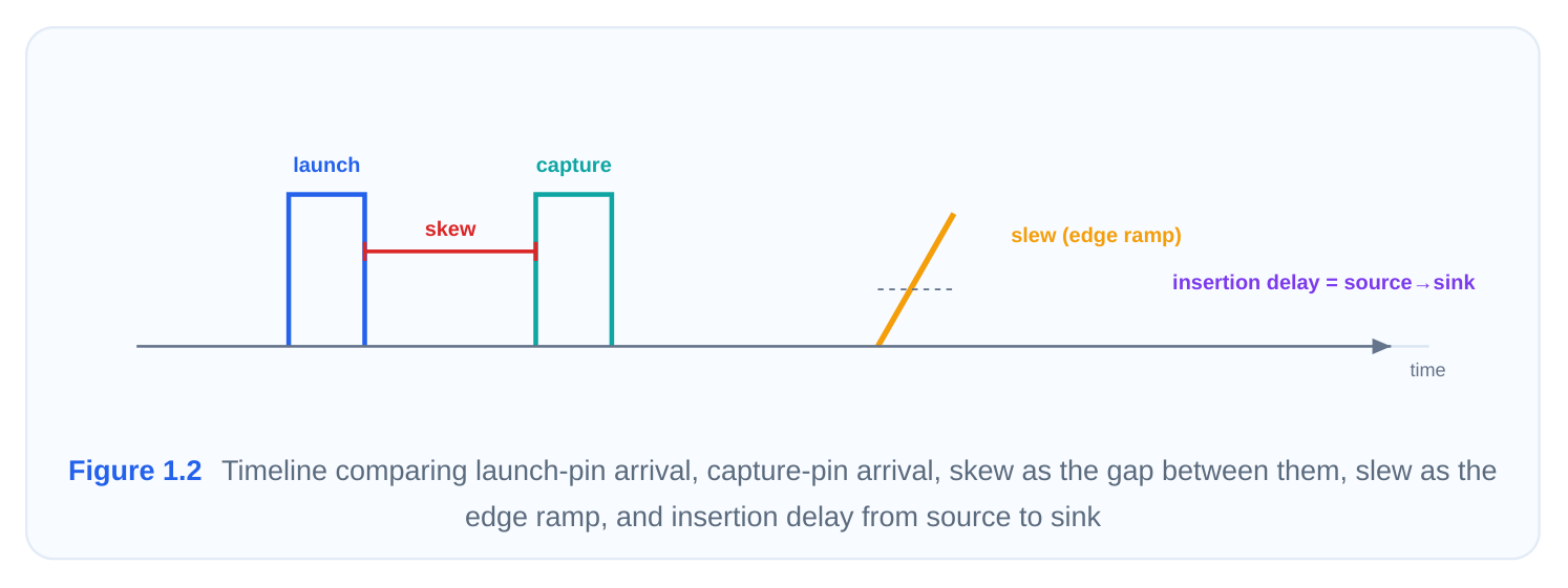
When you sit in a CTS review, three numbers dominate the conversation. Defining each precisely is exactly the kind of thing an interviewer probes. Clock skew. Skew is the difference in clock arrival time between two endpoints. For a launch flop and a capture flop, skew = (arrival time at capture clock pin) − (arrival time at launch clock pin). It is a relative measurement between two points, not an absolute delay. Global skew refers to the spread between the earliest and latest arriving sinks across the whole tree; local skew refers to the difference between specific related register pairs that actually communicate. Note that skew is not inherently bad — useful skew deliberately steers clock arrival to borrow time between stages and help timing — but uncontrolled skew is a primary cause of both setup and hold failures. Clock slew (transition time). Slew is how long the clock signal takes to change state — the rise time and fall time of the clock edge, usually measured between defined voltage thresholds (commonly 9%– 88% or 18%–78% of the supply). A sharp, fast slew is desirable. Slow slews increase delay uncer‐ tainty, make the clock more sensitive to noise and on-chip variation, and waste short-circuit power inside the receiving gates. CTS enforces a maximum transition target at every node so no clock pin ever sees a sluggish edge. Insertion delay / latency. Insertion delay (also called clock latency) is the absolute time the clock takes to travel from the source to a given sink. Two flavors matter: source latency, the delay from the true clock origin to the clock-definition point (often the port or PLL output), and network latency, the delay through the tree itself from that point to the leaf. Total latency is their sum. Lower insertion delay is generally better because it reduces the design's exposure to on-chip variation — a long latency path
accumulates more variation, which inflates the uncertainty you must budget against in both setup and hold checks.
A compact way to remember the relationships:
| Metric | What it measures | Reference | Goal |
|---|---|---|---|
| Skew | Arrival-time difference between two sinks | Relative (point-to- point) | Minimize (or apply useful skew in‐ tentionally) |
| Slew | Edge transition time at a node | Voltage thresholds | Keep under max-transition target |
| Insertion | Source-to-sink absolute delay | Absolute | Minimize to limit OCV exposure |
delay
1.3 CTS in the Design Flow
CTS does not stand alone. It sits in a precise position in the implementation flow, with strict expectations about what must be true before it starts and what it must hand off afterward. Understanding that context is what separates an engineer who runs CTS from one who owns it.
Pre-CTS: getting to a clean starting point
The work that feeds CTS begins far upstream:
- 1. RTL design describes behavior in Verilog/VHDL, with the clocking architecture (number of clocks,
domains, gating scheme) decided here.
- 2. Logic synthesis maps the RTL to standard cells, optimizing for an ideal clock. The synthesized
netlist defines how many flip-flops exist and therefore how many sinks the tree must reach.
- 3. Floorplanning fixes die size, macro placement, power grid, and I/O — the physical canvas the tree
must live on.
- 4. Placement positions every standard cell. Crucially, placement assumes an ideal clock, so timing
here is preliminary. By the time CTS begins, you want the placement to be legal, the power grid in place, and the design free of obvious congestion hotspots. A few specific preconditions matter a great deal: clock definitions
( create_clock , generated clocks, clock-gating cells) must be correct and complete; clock sources must be identified; non-default routing rules and the list of approved clock buffers/inverters must be ready; and any NDR (non-default routing) or shielding intent should be defined. Garbage in, garbage out applies forcefully here — a missing generated clock or an unmarked clock-gating cell will produce a malformed tree.
The CTS stage itself: define → verify → synthesize → optimize
Within the CTS step, the work proceeds through four conceptual phases. Define. You specify the targets and constraints: skew and latency goals, maximum transition, maxim‐ um capacitance and fanout, the cell list the tool may use, routing rules, and which pins are sinks versus which should be excluded (for example, ignore pins or pre-existing clock structures). This is where engineering intent becomes machine-readable.
# Define the clock tree synthesis specification
create_clock -name CLK -period 2.4 [get_ports clk_in]
set_clock_tree_options -clock_trees CLK \
-target_skew 0.036 \
-target_early_delay 0.0 \
-max_capacitance 0.135 \
-max_transition 0.110 \
-max_fanout 28
# Restrict CTS to qualified, characterized cells only
set_lib_cell_purpose -include cts \
[get_lib_cells {*/CLKBUF_X* */CLKINV_X* */CLKBUFHD_X*}]
Verify. Before committing, the tool (and the engineer) check that the specification is self-consistent and physically achievable: are the targets reasonable for the floorplan, are all sinks reachable, are the cell lists valid, are there conflicting constraints? Catching an over-aggressive skew target or an unreachable sink here saves a wasted multi-hour run. Synthesize. This is the construction step. The tool builds the actual tree — choosing where to insert buffers and inverters, how to branch, and how to route the clock nets — to satisfy the targets. Algorithms balance the load down each branch so that the arrival times converge. Optimize. After the initial tree exists, the tool refines it: resizing buffers, adjusting branch points, balancing latency across domains, and running concurrent clock-and-data optimization where the data path and the clock are tuned together. Modern flows fold post-CTS timing optimization (setup/hold fixing with the now-propagated clock) into this phase.
# Build and then optimize the tree, then check the result
clock_opt -from build_clock -to route_clock
# Switch from ideal to propagated clock for real timing
set_propagated_clock [all_clocks]
# Sanity-check skew, latency, and transition outcomes
report_clock_tree   -summary
report_clock_timing -type skew
report_clock_timing -type latency
Post-CTS: routing, DFM, and sign-off
Once the tree is built and timing is recovered, the flow continues:
- 1. Detailed routing completes all remaining (data) nets around the now-fixed clock routing. The clock
is usually routed first and protected, so signal routing must work around it.
- 2. Post-route optimization repairs timing and DRCs introduced by real routing parasitics.
- 3. DFM / physical verification runs DRC, LVS, antenna checks, and design-for-manufacturability
fixes (via doubling, wire spreading, metal fill).
- 4. Sign-off performs final static timing analysis with extracted parasitics and OCV/AOCV/POCV
models, plus power, IR-drop, and EM checks — all with the propagated clock as the source of truth. The clean handoff is the point: CTS converts an idealized design into one whose clock behaves like silicon, so that everything downstream is analyzing reality.
| Flow stage | Clock model | What CTS guarantees / consumes |
|---|---|---|
| Pre-CTS (synth, place) | Ideal | Provides legal placement + complete clock |
definitions
| CTS (define→optimize) | Transitioning to propag‐ | Builds balanced, slew-clean tree; recovers tim‐ |
|---|---|---|
| ated | ing | |
| Post-CTS (route, DFM, sign- | Propagated | Hands off real latency/skew for final closure |
off)
1.4 Design Philosophy: Systemic Precision
CTS is sometimes taught as a checklist of commands, but the engineers who consistently produce good trees think about it as a system-design discipline. Three principles capture that mindset.
Hierarchical information architecture
A clock tree is, at its heart, an information-distribution network, and the best ones obey the same principles as any well-architected hierarchy: information (here, the clock edge) flows from a single authoritative source, fans out through orderly, predictable levels, and arrives everywhere with a known, bounded quality of service. Each level of the tree has a clear responsibility — early levels carry the signal across distance, middle levels balance major regions, and leaf levels deliver clean edges to sinks. When the hierarchy is clean, you can reason about the whole network by reasoning about one level at a time. When it is muddled — when branches cross, when latencies between siblings diverge wildly, when buffers are sized inconsistently — the tree becomes opaque, hard to debug, and fragile under variation. Designing for a legible hierarchy is not aesthetic preference; it is what makes the network analyzable and repairable.
Minimal-text, expert craftsmanship
A second principle is restraint. The strongest CTS results usually come from doing less, not more: few‐ er buffer levels, the minimum insertion delay that meets slew, the smallest cell that satisfies the load, and no redundant balancing structures. Every extra buffer is extra power that toggles every cycle, extra area, extra variation, and one more thing that can fail. Expert craftsmanship in CTS looks like a spare, deliberate tree where each element earns its place — much like clean, minimal code. This restraint also shows up in how you write constraints: a tight, well-chosen specification (a sensible skew target, a realistic max-transition, a curated cell list) guides the tool toward elegant solutions, whereas an over-specified, contradictory constraint set forces it into baroque, over-buffered compromises.
Well-organized distribution networks
Finally, treat the clock network as infrastructure to be organized, not noise to be tolerated. That means routing the clock on appropriate metal layers with non-default rules for lower resistance, considering shielding to protect against crosstalk on the most timing-critical nets, placing buffers on a regular structure rather than scattering them, and keeping related sinks grouped so that local skew between communicating registers stays naturally small. A well-organized network is also a predictable one: when the next engineer (or the next ECO) touches the block, an orderly tree behaves predictably, while a chaotic one produces surprises. Good CTS, in other words, is an act of stewardship — you are building a piece of infrastructure that the rest of the chip, and the rest of the team, will rely on. These philosophies converge on a single idea: systemic precision. The clock is the one signal the entire synchronous design trusts implicitly, so the network that carries it should be built with the discipline of critical infrastructure — hierarchical, minimal, organized, and predictable.
Interview Q&A
change? An ideal clock assumes zero delay and zero transition at every sink, which is physically
impossible and makes pre-CTS timing optimistic. CTS replaces that assumption by inserting real buffers and routing real wires, producing a propagated clock with genuine insertion delay, skew, and slew. After CTS, the timing engine analyzes actual arrival times, so setup and hold checks reflect silicon behavior. Without it, you would be signing off on timing that the physical clock can never deliver.
the difference in clock arrival time between two sinks — it is a relative, point-to-point measurement. Slew is the transition (rise/fall) time of the clock edge at a node, measured between voltage thresholds. Insertion delay (latency) is the absolute time from the clock source to a given sink, split into source latency and network latency. Skew drives setup/hold margins between register pairs; slew affects delay accuracy and power; insertion delay governs how much on-chip variation the path accu‐ mulates.
The clock distribution network typically consumes about 18–37% of dynamic power and occupies around 4–13% of cell area. The power is high because the clock toggles every cycle — far more than any data net — across a large number of buffers and long, high-fanout wires. The area is significant because building a balanced tree to thousands or millions of sinks requires many buffers and inverters plus dedicated routing tracks on preferred metal layers.
lows RTL, synthesis, floorplanning, and placement, and precedes detailed routing, DFM, and sign-off. Before it runs, placement must be legal, the power grid in place, and crucially all clock definitions must be complete and correct — primary clocks, generated clocks, clock-gating cells, identified sources, the approved CTS cell list, and any non-default routing or shielding intent. Internally CTS proceeds define → verify → synthesize → optimize, then the clock is set propagated and timing is recovered before handing off to routing.
Key Takeaways
- CTS builds the real, hierarchical buffer-and-wire tree that delivers the clock from a single source to every clocked endpoint, replacing the ideal-clock assumption with a propagated one.
- It is a top-tier flow step because it simultaneously determines timing closure, dynamic power (~18– 37% of the total), and clock area (~4–13% of cell area).
- The three metrics to master are skew (relative arrival-time difference), slew (edge transition time), and insertion delay/latency (absolute source-to-sink delay).
- CTS sits between placement and routing and runs through define → verify → synthesize → optim‐ ize, transitioning the clock from ideal to propagated so downstream stages analyze reality.
- A good tree is built with systemic precision: a legible hierarchy, minimal and deliberate buffering, and a well-organized, predictable distribution network that the rest of the chip can trust.
Comments
Leave a Reply