 ChipBuddy
← Home
ChipBuddy
← Home
Defining Clock Trees
Before a single clock buffer can be placed or a skew number computed, the tool has to answer a deceptively simple question: what, exactly, is the clock tree? That means knowing where the clock comes from, every register it must reach, which pins it must drive and which it must deliberately ignore, and how the structure should look between source and sinks. Getting this definition wrong is one of the most common reasons CTS produces a "correct" tree that still fails timing — the tool optimized the wrong network. This topic walks through how a clock network is derived, how roots and endpoints are recognized, how the source is modeled electrically, how legacy cells already sitting in the path are absorbed, and how trees that fan in from several sources are reconciled.
5.1 Deriving the Clock Trees
A clock tree is not something you draw by hand; the implementation tool derives it by walking the netl‐ ist. The process begins at a declared clock source and follows the signal forward through the design, collecting every cell and net the clock edge can physically reach. This forward walk is called transitive fanout tracing.
Transitive fanout tracing
Transitive fanout means "the fanout of the fanout of the fanout…" — you keep expanding outward until you hit something that stops the trace. Starting at the clock root, the tool looks at the net driven by that pin, finds every load pin on it, then for each load that is a combinational element (a buffer, inverter,
AND/OR gate, MUX, clock gate) it continues forward through that cell's output. The walk halts at three natural boundaries:
- A sequential element's clock pin (the CK pin of a flop or latch) — this is a leaf of the tree.
- A macro or hard-IP clock input that the tool treats as a sink.
- A pin the engineer has explicitly marked to stop propagation (an ignore pin or a generated-clock boundary). Everything gathered along the way — the buffers, the gating cells, the nets — constitutes the clock tree for that source.
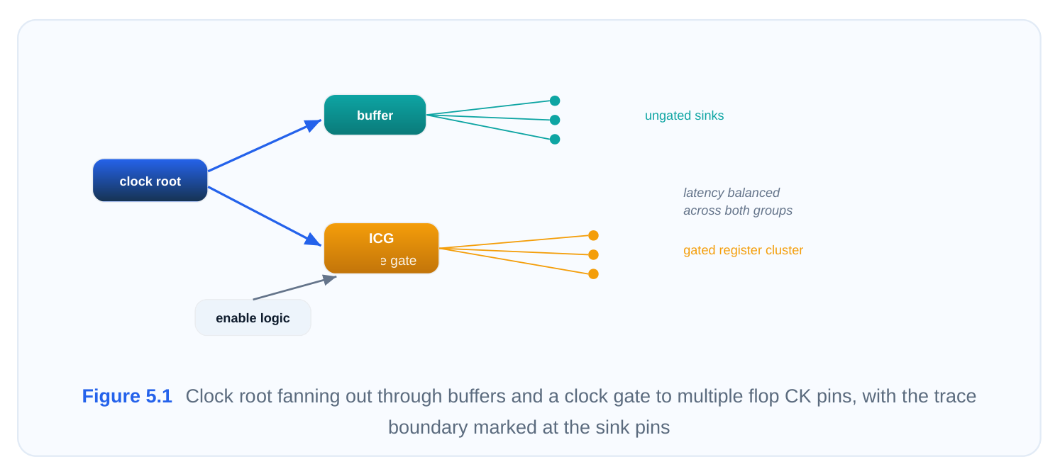
Clock-root identification and endpoint derivation
Two outputs fall directly out of the trace. The root is the pin the trace started from. The endpoints (sinks) are the pins where the trace terminated on sequential clock inputs. Sections 5.2 and 5.3 cover each in detail, but the key idea is that both are consequences of how clocks are defined plus how the netlist is wired — the tool computes them, the engineer mostly verifies and corrects them.
Clock-gating logic analysis
Most real designs gate their clocks for power. An integrated clock-gating cell (ICG) sits in the clock path and only lets edges through when an enable is asserted. From the tree-derivation point of view, the ICG is simply a cell the trace passes through: the clock enters on the gate's clock input, and the trace continues from the gate's gated clock output to the downstream flops. The enable input is a data pin, not a clock pin, so the trace does not propagate backward into the enable logic. CTS still has to balance the latency up to and through the gate so that gated and ungated branches stay aligned — but for derivation purposes, the ICG is just another in-line cell on the path.
Non-unate cells: XOR / XNOR handling
Here is a subtlety interviewers love. Most clock-path cells are unate — a rising edge in produces a predictable rising or falling edge out (buffers are positive-unate, inverters negative-unate). An XOR or XNOR gate is non-unate: whether a transition on one input shows up rising or falling at the output depends on the state of the other input. When the clock routes through such a gate (common in test logic, clock muxing, or divide-by-two structures built from XORs), the tool cannot assign a single, consistent sense to the propagated clock. It must consider both polarities, which can double the timing checks and confuse skew analysis if left unmanaged. The practical guidance is to keep clocks out of non-unate gates when you can, and where you cannot, define the clock such that the "other" input is held at a known constant (a set_case_analysis ) so the gate behaves unately for that mode.
| Cell type | Unateness | Effect on clock sense |
|---|---|---|
| Buffer | Positive-unate | Edge polarity preserved |
| Inverter | Negative-unate | Edge polarity flipped, but deterministic |
| AND/OR (one pin = | Unate (with side pin con‐ clock) | Deterministic if side pin fixed stant) |
| XOR / XNOR | Non-unate | Output edge depends on side-pin state; both senses |
considered
5.2 Identifying Clock Roots
The root is the origin point of a clock tree. Every clock has exactly one root, but a design has many roots, and they show up in several flavors. Knowing where roots can legitimately live is essential when you debug a missing or mis-rooted clock.
Input-port clock sources
The most common root is a top-level input port — the clock arrives from a PLL or board oscillator outside the block and enters through a primary input. You declare it with create_clock on that port. The tool then traces forward from the port into the design.
Internal hierarchical pins
A root does not have to be a primary input. You can anchor a clock on an internal pin — for example, the output of a clock divider, the output pin of a PLL macro inside the block, or a hierarchical boundary pin. This is essential when the clock-generating logic is part of your block rather than upstream of it.
create_clock-defined roots
Any object you name in a create_clock command becomes a root. The command is what tells the tool "treat this point as a clean clock source with the following waveform." Without it, the tool has no waveform and cannot derive timing for the network.
# Root on a top-level input port
create_clock -name CLK_SYS -period 2.6 [get_ports clk_in]
# Root on an internal pin (e.g., PLL output buffer)
create_clock -name CLK_CORE -period 1.2 [get_pins pll_inst/CLKOUT]
Nested roots
Sometimes a clock defined deeper in the design sits inside the fanout of another clock — a clock cre‐ ated on an internal pin that is itself reachable from an upstream port clock. This is a nested root. By convention the most recently / most locally defined clock wins on that pin and downstream: the inner
create_clock overrides the propagation of the outer one past that point. This is how you intentionally"cut" one clock and start a fresh one — useful when an upstream clock should not be balanced together with the downstream domain.
Generated-clock master sources
A generated clock is derived from another clock — a divide-by-two, a multiplied PLL output, a gated version — and is defined relative to a master source pin. The generated clock's root is its own defini‐ tion pin, but its timing characteristics (waveform, edges) are inherited and transformed from the master. When you identify roots, you must distinguish a true create_clock root (a standalone source with its own waveform) from a create_generated_clock root (a dependent source that tracks a mas‐ ter).
# Master clock
create_clock -name CLK_REF -period 2.4 [get_ports ref_clk]
# Divide-by-2 generated clock, rooted on the divider's Q output
create_generated_clock -name CLK_DIV2 \
-source [get_ports ref_clk] -divide_by 2 \
[get_pins div_reg/Q]| Root type | Defined by | Has own waveform? | Typical location |
|---|---|---|---|
| Port clock | create_clock | Yes | Primary input port |
| Internal source | create_clock | Yes clock | Internal pin (PLL/divider out) |
| Nested clock | create_clock inside another's | Yes (overrides up‐ fanout | Internal pin stream) |
| Generated clock | create_generated_clock | No (derived from master) | Divider/multiplier output pin |
5.3 Identifying Clock Endpoints
Endpoints are where the tree terminates. CTS treats each endpoint as either a point it must balance to (a sink) or a point it must leave alone (an ignore pin). Misclassifying even one endpoint is enough to skew the whole tree, so this step deserves real attention.
Sink pins vs ignore pins
A sink pin is an endpoint CTS is responsible for: a flop CK pin, a latch enable, a macro clock input — anything that needs clock delivered with controlled latency and skew. CTS includes it in the balancing target set. An ignore pin is an endpoint CTS deliberately excludes from balancing. Classic examples: the clock feeding a divider whose output is its own clock domain (you don't want it balanced against the divided domain), a clock observation point used only for test, or a sink whose timing is checked under a different mode. The clock still physically reaches an ignore pin, but the tool does not try to equalize its arrival time with the real sinks.
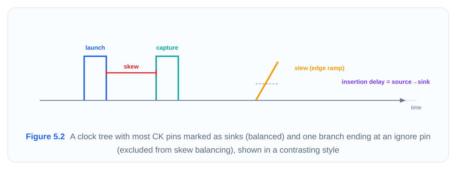
Automatic vs manual classification
The tool performs a default automatic classification: any flip-flop/latch clock pin reached by the trace is taken as a sink, while structures like the clock input of a flop that generates a new (nested/ generated) clock are flagged as ignore/stop points automatically. You then manually override where the auto-classification is wrong — for example, marking a particular sink as an exception or promoting an ignore pin back to a sink.
# Mark a pin as a sink the tool should balance to
set_clock_tree_options -clock CLK_CORE ...
# Treat a leaf as a non-stop / ignore endpoint (tool-specific syntax)
set_ccopt_property sink_type stop -pin_list [get_pins div_reg/CK]
set_ccopt_property sink_type ignore -pin_list [get_pins scan_obs/CK]
Default endpoint types
It helps to keep a mental table of the default sink categories a modern CTS engine recognizes:
| Endpoint type | Default treatment | Balanced for skew? |
|---|---|---|
| Flop / latch clock pin | Sink | Yes |
| Macro / IP clock input | Sink (with insertion-delay offset) | Yes, with offset |
| Pin generating a nested clock | Stop | No (new domain starts here) |
| Test / observe-only pin | Ignore | No |
| Floating / unconnected reach | Ignore | No |
The "stop" versus "ignore" distinction matters: a stop pin still anchors a domain boundary (a new clock continues beyond it), while an ignore pin is genuinely dropped from the optimization. Confusing the two leads to either an unbalanced downstream domain or wasted effort balancing something nobody checks.
5.4 Specifying Clock Root Timing Characteristics
Deriving the structure tells you what the tree is; specifying root timing tells the tool how the clock actu‐ ally arrives at the source. If you skip this, the tool assumes an ideal, infinitely strong, zero-transition clock — and then builds a tree tuned to a fantasy. The result fails in silicon because the real driver is weaker and slower.
Input-port driving-cell specification
For a clock that enters on a port, you tell the tool what is driving that port on the other side of the boundary with set_driving_cell . This attaches a real library cell's output characteristics to the port, so the input transition the tool sees is realistic rather than ideal.
# Model the off-block driver of the clock port as a real buffer
set_driving_cell -lib_cell BUFX8 -pin Z [get_ports clk_in]
# Optionally model a known external transition directly
set_input_transition 0.08 [get_ports clk_in]
Pad-cell modeling
When a clock comes in through an I/O pad, the pad cell itself has meaningful delay and a characterist‐ ic output slew. Modeling the pad (either by including the actual pad cell in the path or by using a driving-cell that represents it) ensures the latency budget accounts for the pad's contribution. Forgetting the pad is a common reason measured insertion delay overshoots the plan.
Weak vs strong driver impact
The strength of the assumed driver changes everything downstream:
- A strong driver produces a sharp input transition. The tool sees a fast edge, predicts low delay at the first stage, and may insert fewer / smaller buffers near the root.
- A weak driver produces a slow, degraded edge. The tool sees a sluggish transition, predicts higher delay, and compensates by inserting more or larger buffers early to recover slew. If you model the driver as stronger than reality, CTS under-buffers the root, real transitions are slow, and you get unexpected delay and duty-cycle distortion. Modeling it weaker than reality over-buffers and wastes area/power. The goal is realistic, not optimistic.
Buffer-insertion consequences and realistic timing models
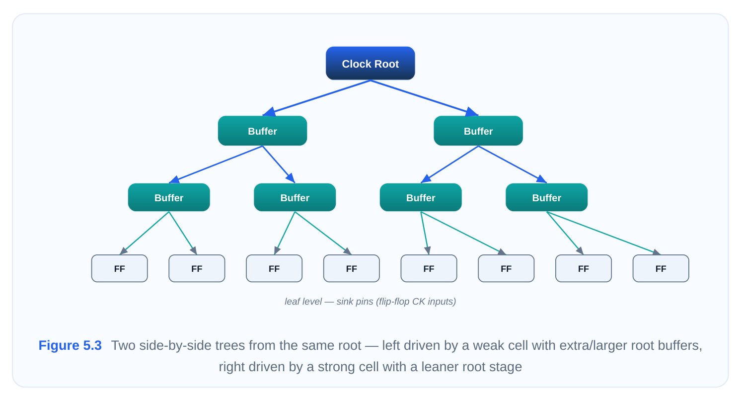
The driving-cell choice directly seeds the first-stage buffer plan, the achievable transition target, and therefore the entire latency profile. A realistic timing model at the root — correct driver strength, correct external transition, pad delay included, with the right operating corner — is the single most leverageheavy input to a clean CTS run. Treat the root spec as part of the constraint quality review, not an af‐ terthought.
5.5 Pre-existing Cells in the Clock Tree
CTS rarely starts from a perfectly clean slate. The incoming netlist often already contains buffers and inverters on the clock path — placed by synthesis, carried over from a previous block, or handinstantiated for a specific reason. The tool has to decide what to do with them.
Handling existing buffers
When CTS encounters cells already sitting on the clock path, it can take one of three stances:
- 1. Absorb and re-optimize — treat the existing cells as ordinary clock-path cells, free to resize,
relocate, or delete them as it builds the optimal tree. This is the default for most ordinary synthesis buffers.
- 2. Preserve (don't touch) — keep specific cells exactly as-is because they were placed deliberately
(an inverter pair for duty-cycle correction, a specific delay element, a cell tied to a particular physical location). You protect them with a don't-touch attribute.
- 3. Replace — swap an existing cell for a more suitable clock-tree cell from the dedicated clock library
(e.g., a balanced-rise/fall clock buffer instead of a generic data buffer).
# Protect a deliberately placed inverter pair from CTS modification
set_dont_touch [get_cells {clk_path/inv_a clk_path/inv_b}] true
# Allow the rest of the path to be re-optimized (leave un-touched -> default)
Reuse vs replacement
The decision hinges on why the cell exists. If it is a generic buffer that synthesis dropped in just to fix a transition, let CTS replace or remove it — the CTS engine will do a better, placement-aware job. If the cell encodes intent CTS cannot infer (matched delay across a custom interface, a specific cell type required by a hard macro, a manually balanced leg), reuse it and lock it down. A useful rule of thumb: reuse what carries intent, replace what carries only a quick fix.
Topology integration
Whatever is preserved must be folded into the derived topology cleanly. A locked inverter on one leg, for instance, flips polarity on that branch — the tool must account for that when balancing sinks downstream, possibly adding a matching inversion on sibling legs. Pre-existing cells therefore are not just "kept"; they become fixed constraints the new tree must build around. Reviewing the path for un‐ expected don't-touches before CTS is a good habit; a stray don't-touch buffer is a frequent cause of a leg the tool mysteriously refuses to optimize.
5.6 Clock Tree Convergence
Convergence describes how branches relate to sources — specifically, whether each sink is fed by exactly one source or by several. Modern clock-concurrent engines handle more than the simple textbook case, and interviews probe whether you understand the variants.
Single-source trees
The classic case: one root, fanning out through a hierarchy of buffers to many sinks, with no branch ever fed by a second source. This is the easiest to balance because every sink has exactly one latency path back to the root, so skew is just the spread of those path delays.
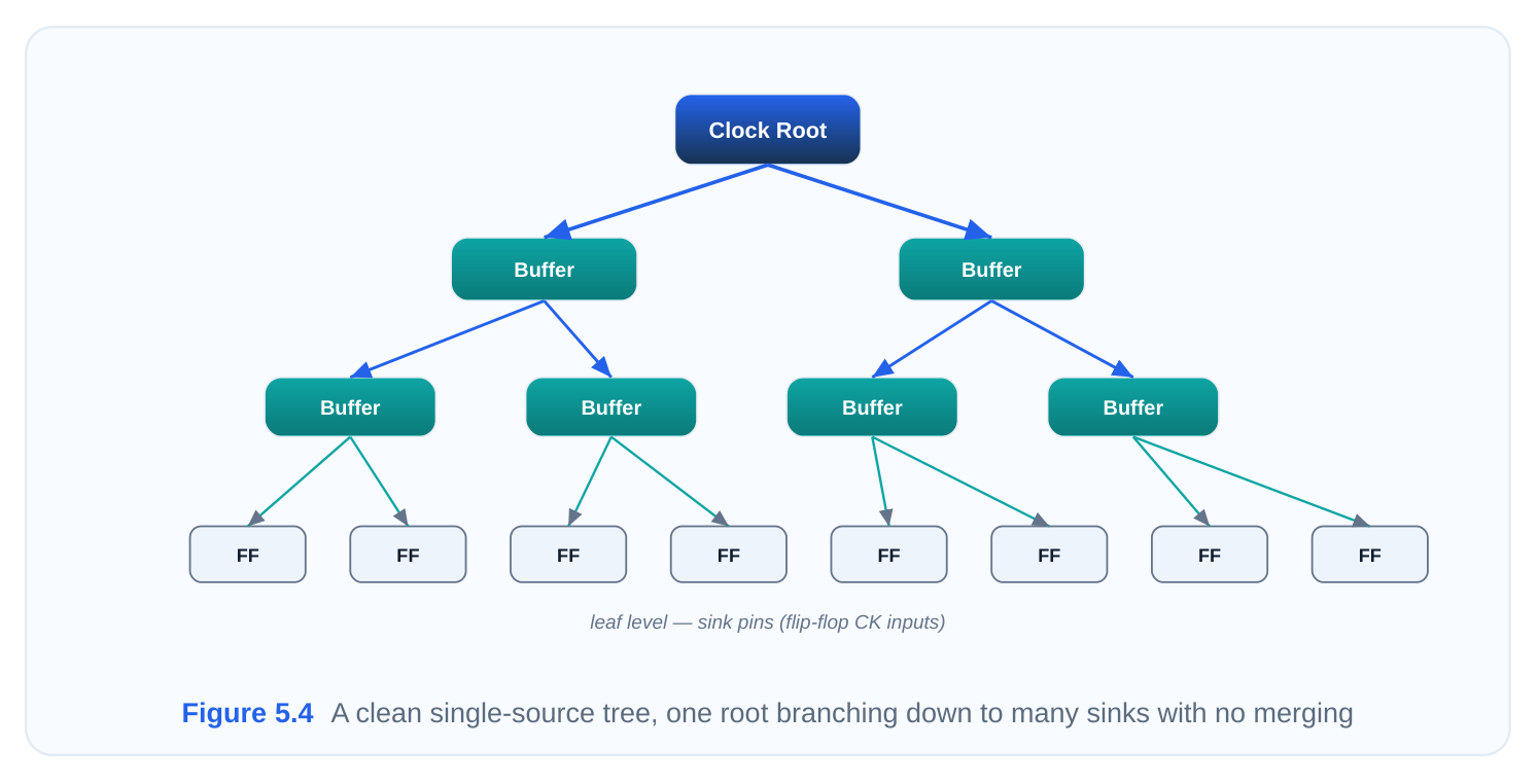
Multi-source trees
In a multi-source (or mesh/spine-fed) structure, several drivers cooperate to deliver the same clock to a region — for example, a clock mesh where a grid of drivers is shorted together, or multiple top-level taps driving one sub-block. The advantage is dramatically lower skew and better tolerance to on-chip variation, because the shorted network averages out individual driver delays. The cost is much higher power and routing resource, plus harder timing analysis (a sink can be driven by many drivers at once). High-performance CPUs and GPUs frequently use mesh or spine-and-mesh hybrids in their most timing-critical regions.
| Aspect | Single-source tree | Multi-source / mesh |
|---|---|---|
| Drivers per sink | One | Many (shorted) |
| Skew | Moderate, depends on balance | Very low |
| OCV tolerance | Lower | High (averaging) |
| Power / routing | Economical | High |
| Analysis complexity | Simple | Complex (multi-driver) |
| Typical use | General SoC blocks | High-perf CPU/GPU cores |
Integrated tap assignment
When a region is fed from a shared upper-level structure (a spine, a mesh, or a set of distribution taps), the tool must decide which tap each sub-tree connects to. Good tap assignment groups physically nearby sinks onto the same tap so each local sub-tree is short and well-balanced, and it spreads load evenly across taps so no single tap is overloaded. Poor tap assignment forces long local routes and reintroduces the skew the mesh was meant to remove. Integrated tap assignment means
the CTS engine chooses these connection points as part of building the local trees, rather than treat‐ ing them as a fixed pre-decided input.
Convergence patterns
Putting it together, the common patterns you should be able to name:
- Pure tree — single source, no convergence; simplest, lowest power.
- Spine + trees — a balanced spine distributes to multiple local trees via taps; a middle ground.
- Mesh / grid — fully convergent, many-to-many; lowest skew, highest cost.
- Hybrid (spine-and-mesh) — mesh over the critical core, trees for the periphery; the pragmatic high-performance choice.
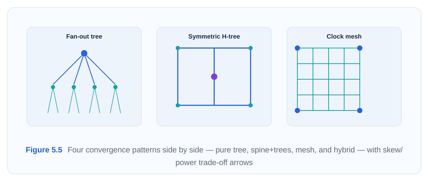
Choosing a pattern is a deliberate trade between skew, power, area, and analysis effort. Most SoCs default to trees and reserve mesh structures for the handful of regions where the skew budget genuinely demands it.
Interview Q&A
is non-unate: the polarity of the edge it produces depends on the logic state of its other input, so the tool cannot assign a single consistent clock sense through it. It must analyze both rising and falling possibilities, which inflates timing checks and muddies skew analysis. The fix is usually to fix the side input to a known constant via set_case_analysis for the relevant mode so the gate behaves unately, or to route the clock around such gates entirely.
halt the forward trace, but they mean different things. A stop pin marks a domain boundary where a new clock (nested or generated) takes over downstream — the tree continues, it just belongs to a different clock from that point on. An ignore pin is genuinely dropped from balancing: the clock
reaches it but the tool makes no attempt to equalize its arrival with the real sinks. Stop pins protect domain integrity; ignore pins exclude irrelevant or separately-checked endpoints.
transition the tool assumes at the source. A weak driver gives a slow edge, prompting the tool to insert more/larger buffers early; a strong driver gives a sharp edge and a leaner root stage. If you model the driver optimistically, CTS under-buffers the root and the real, slower edges cause unexpected delay and duty-cycle distortion in silicon. A realistic root model — correct driver strength, external transition, pad delay, and corner — is one of the highest-leverage inputs to a clean CTS result.
Keep it when it encodes intent the tool cannot infer — a duty-cycle-correction inverter pair, a matched delay element, a cell type a macro requires, or a manually balanced leg — and lock it with a don'ttouch so the new topology builds around it. Let CTS replace or remove it when it is just a generic synthesis buffer dropped in to patch a transition, since the placement-aware CTS engine will optimize it better. The guideline: reuse what carries intent, replace what carries only a quick fix.
Key Takeaways
- A clock tree is derived, not drawn: the tool traces transitive fanout from a declared root forward to sequential clock pins, passing through buffers and clock gates and stopping at sinks and boundar‐ ies.
- Roots come in several forms — port clocks, internal-pin clocks, nested clocks, and generated clocks — and only
create_clock/create_generated_clockgive the tool the waveform it needs. - Endpoints split into sinks (balanced), stop pins (domain boundaries), and ignore pins (excluded); misclassifying even one corrupts the whole tree, so verify the auto-classification.
- Non-unate cells (XOR/XNOR) break the single-clock-sense assumption; constrain their side inputs or avoid them in clock paths.
- Modeling the root's real driver strength, transition, and pad delay is decisive — an optimistic root spec produces a tree that fails in silicon.
- Convergence ranges from simple single-source trees to power-hungry, ultra-low-skew meshes; pick the pattern that matches each region's skew budget, and reuse pre-existing cells only when they carry real design intent.
Comments
Leave a Reply