 ChipBuddy
← Home
ChipBuddy
← Home
Chapter 15 Interfacing to the Analog World
OUTLINE
15–1 Digital and Analog Representations
15–2 Operational Amplifier Basics
15–3 Binary-Weighted D/A Converters
15–4 R/2R Ladder D/A Converters
15–5 Integrated-Circuit D/A Converters
15–6 Integrated-Circuit Data Converter Specifications
15–7 Parallel-Encoded A/D Converters
15–8 Counter-Ramp A/D Converters
15–9 Successive-Approximation A/D Conversion
15–10 Integrated-Circuit A/D Converters
15–11 Data Acquisition System Application
15–12 Transducers and Signal Conditioning
OBJECTIVES
Upon completion of this chapter, you should be able to do the following:
- Perform the basic calculations involved in the analysis of operational amplifier circuits.
- Explain the operation of binary-weighted and R/2R digital-to-analog converters.
- Make the external connections to a digital-to-analog IC to convert a numeric binary string into a proportional analog voltage.
- Discuss the meaning of the specifications for converter ICs as given in a manu- facturer’s data manual.
- Explain the operation of parallel-encoded, counter-ramp, and successive- approximation analog-to-digital converters.
- Make the external connections to an analog-to-digital converter IC to convert an analog voltage to a corresponding binary string.
- Discuss the operation of a typical data acquisition system.
INTRODUCTION
Most physical quantities that we deal with in this world are analog in nature. For example, temperature, pressure, and speed are not simply 1s and 0s but, instead, take on an infinite number of possible values. An illustration of analog-to-digital and digitalto-analog conversions used in music reproduction was given in Figures 1–2 and 1–3.
representing their value; thus, we have the need for analog-to-digital conversion. Also, it Discussion is important when we need to use a computer to control analog devices to be able to con-
| vert from digital to analog. | What are some scientific |
|---|---|
| Devices that convert physical quantities into electrical quantities are called | and commercial |
| transducers. Transducers are readily available to convert such quantities as tempera- | applications for analog- |
| ture, pressure, velocity, position, and direction into a proportional analog voltage or | to-digital conversion |
| current. For example, a common transducer for measuring temperature is a thermistor. | and digital-to-analog |
| A thermistor is simply a temperature-sensitive resistor. As its temperature changes, so | conversion? |
does its resistance. If we send a constant current through the thermistor and then measure the voltage across it, we can determine its resistance and temperature.
15–1 Digital and Analog Representations
For analog-to-digital (A/D) or digital-to-analog (D/A) converters to be useful, there has to be a meaningful representation of the analog quantity as a digital representation and the digital quantity as an analog representation. If we choose a convenient range of analog levels such as 0 to 15 V, we could easily represent each 1-V step as a unique digital code, as shown in Figure 15–1.
| Analog voltage (V) | 11 | ||||||||||
|---|---|---|---|---|---|---|---|---|---|---|---|
| 1 | 2 | 3 | 4 | 5 | 6 | 7 | 8 | 9 | 10 | 11 | 12 |
Time (ms) (a) Representation
| Time (ms) | Analog | Digital | |||
|---|---|---|---|---|---|
| 1 | 3 | 0011 | |||
| 2 | 5 | 0101 | |||
| 3 | 9 | 1001 | |||
| 4 | 10 | 1010 | |||
| 5 | 13 | 1101 | |||
| 6 | 14 | 1110 | |||
| 7 | 13 | 1101 | D0 | ||
| 8 | 11 10 V | 1011 1 | D1 | ||
| 9 | 10 Analog | 1010 D2 | 4-bit A/D | Digital | |
| 10 | 10 | 1010 | converter | 0 | out |
in
| 11 | 8 | 1000 | D3 |
|---|---|---|---|
| 12 | 5 | 0101 (b) Figure 15–1 | 1 (c) Analog and digital representations: (a) voltage versus time; (b) representations |
at 1-ms intervals; (c) results at the 4 ms time.
digital representation. For example, at 4 ms the analog voltage of 10 V will be represented by an A/D converter as 10102. Using four binary positions gives us 4-bit resolution, which allows us to develop 16 different representations, with the increment between each being 1 part in 16. If we need to represent more than just 16 different analog levels, we would have to use a digital code with more than four binary positions. For example, a D/A converter with 8-bit resolution will provide increments of 1 part in 256, which provides much more precise representations.
15–2 Operational Amplifier Basics
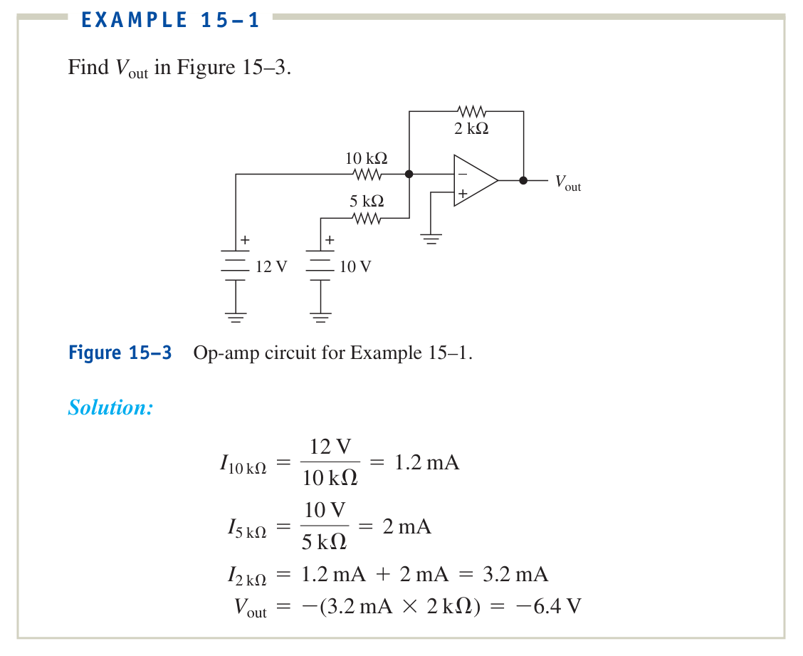
Most A/D and D/A circuits require the use of an op amp for signal conditioning. Three characteristics of op amps make them an almost ideal amplifier: (1) very high input impedance, (2) very high voltage gain, and (3) very low output impedance. In this section, we gain a basic understanding of how an op amp works, and in future sections, we see how it is used in the conversion process. A basic op-amp circuit is shown in Figure 15–2. IF = Ii IF = 0.5 mA
| + | – | |||
|---|---|---|---|---|
| Vi | 5 V | |||
| Ii = | = | = 0.5 mA | RF | Vout equals the |
| Ri | 10 kΩ | |||
| 1 kΩ | voltage across RF |
I = 0
+ –
| Ri | G | Op | Op | Vout = –Vi |
|---|---|---|---|---|
| + | Ri× RF | |||
| Vi | 10 kΩ | I = 0 | amp 5 V – Figure 15–2 | amp + = –(0.5 mA × 1 kΩ) = −0.5 V Basic op-amp operation. |
The symbol for the op amp is the same as that for a comparator, but when it is connected as shown in Figure 15–2, it provides a much different function. The basic theory involved in the operation of the op-amp circuit in Figure 15–2 is as follows:
- 1. The impedance looking into the (+) and (-) input terminals is assumed to
| be infinite; therefore, Iin | (+), | (-) = 0A. |
|---|---|---|
| 2. Point G is assumed to be at the same potential as the | (+) | input; therefore, |
point G is at 0 V, called virtual ground. (Virtual means “in effect” but not actual. It is at 0 V, but it cannot sink current.)
- 3. With point G at 0 V, there will be 5 V across the 10@k� resistor, causing 0.5 mA
to flow.
- 4. The 0.5 mA cannot flow into the op amp; therefore, it flows up through the
1@k� resistor.
to ground, Vout is equal to the voltage across the 1@k� resistor, which is
Review Questions
15–1. Transducers are devices that convert physical quantities like pressure and temperature into electrical quantities. True or false? 15–2. An 8-bit A/D converter is capable of producing how many unique digital output codes? 15–3. The input impedance to an operational amplifier is assumed to be
_________. The voltage difference between the (+) input and (-) input is
15–3 Binary-Weighted D/A Converters
A basic D/A converter (DAC) can be built by expanding on the information presented
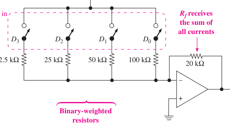
in Section 15–2. Example 15–1 showed us that the 2@k� resistor receives the sum of input resistors with a binary weighting factor, each input can be made to provide a binary-weighted amount of current, and the output voltage will represent a sum of all the binary-weighted input currents, as shown in Figure 15–4.
In Figure 15–4, the 20@k� resistor sums the currents that are provided by closing
| weighted amount of current to be summed by the | 20@k� | resistor. Closing D0 causes | ||||
|---|---|---|---|---|---|---|
| 50 | mA | to flow through the | 20k�, | creating | -1.0V | at Vout. Closing each successive |
switch creates double the amount of current of the previous switch. Work through several of the switch combinations presented in Figure 15–4 to prove its operation. If we were to expand Figure 15–4 to an 8-bit D/A converter, the resistor for D4
| would be one-half of | 12.5k�, | which is | 6.25k�. | Each successive resistor is one-half |
|---|---|---|---|---|
| of the previous one. Using this procedure, the resistor for D7 would be | 0.78125k� | ! |
D3 D2 D1 D0 Vout (–V)
0 0 0 0 0
| 1 | 1 | 1 | 0 | 14 |
|---|---|---|---|---|
| 1 | 1 | 1 | 1 (a) | 15 (b) |
D0
| Digital | D1 | 4-bit D/A | Analog |
|---|---|---|---|
| input | D2 | converter | out |
D3 (c)
Figure 15–4 Binary-weighted D/A converter: (a) circuit diagram; (b) input-output results;
(c) block diagram. Coming up with accurate resistances over such a large range of values is very difficult. This limits the practical use of this type of D/A converter for any more than 4-bit conversions.
EXAMPLE 15–2
Determine the voltage at Vout in Figure 15–4 if the binary equivalent of 1010
Solution: 1010 = 10102 (switches D3 and D1 are closed)
5V
I3 = 12.5k�= 0.4mA
I1 = 50k�= 0.1mA
15–4 R/2R Ladder D/A Converters
The method for D/A conversion that is most often used in D/A converters is known as the R/2R ladder circuit. In this circuit, only two resistor values are required, which lends itself nicely to the fabrication of ICs with a resolution of 8, 10, or 12 bits, and higher. Figure 15–5 shows a 4-bit D/A R/2R converter. To form converters with higher
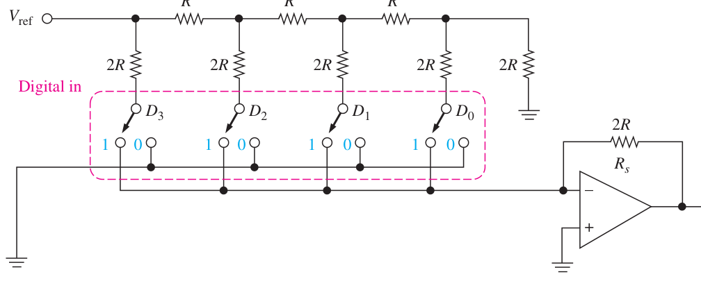
Figure 15–5 The R/2R ladder D/A converter.
resolution, all that needs to be done is to add more R/2R resistors and switches to the left of D3. Commercially available D/A converters with resolutions of 8, 10, 12, 14, and 16 bits are commonly made this way. In Figure 15–5, the 4-bit digital information to be converted to analog is entered on the D0 to D3 switches. (In an actual IC, those switches would be transistor switches.) The arrangement of the circuit is such that as the switches are moved to the
1 position, they cause a current to flow through the summing resistor, Rs, that is proprevious one.) This circuit, which is designed in the shape of a ladder, is an ingenious way to form a binary-weighted current-division circuit. Refer to Figure 15–6(a) to see how we arrive at the current levels and value of Vout. First, keep in mind the op-amp rules pre-
sented in Section 15–2. In particular, remember that the (-) input to the op amp is at
through the summing resistor (Rs). With this knowledge, we can determine that the retion of any of the data switches (D3 to D0). This is because (1) with a data switch in the
0 position, the bottom of the corresponding 20@k� resistor is connected to ground and as ground. Current divides equally
| 500 μA | at each branch | |||||
|---|---|---|---|---|---|---|
| A | 10 kΩ | B | 10 kΩ | C | 10 kΩ | D |
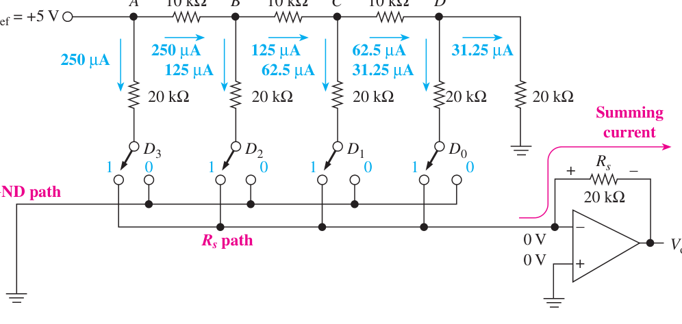
Figure 15–6 R/2R ladder D/A converter: (a) Current division;
SECTION 15–4 | R/2R LADDER D/A CONVERTERS 721
calculate the total current leaving Vref. By collapsing the circuit from the right, we have
| 20k� | in parallel with | 20k�, | which gives | 10k�. | This | 10k� | is in series with the |
|---|---|---|---|---|---|---|---|
| 10@k� | resistor between C and D, making | 20k�. | This | 20k� leaving Vref is 5 V divided by | is now in parallel with the at the total resistance seen by Vref being equal to 10k�, | 20@k� 10k�. which equals | resistor above D1. This procedure is repeated over and over until we arrive Therefore, the total current 500mA. |
When that current reaches point A, it divides equally into the two branches, be-
| cause each branch is | 20k�. | The | 250mA | that reaches point B also splits equally, send- |
|---|---|---|---|---|
| ing | 125mA | down the D2 rung. This current splitting continues for each rung. Notice |
that each resulting current is one-half the current to its left, forming a binary-weighted ratio that is then available for the op-amp summing resistor.
| If D3 is in the 1 position, the | 250mA | is routed through the | 20@k� | summing |
|---|---|---|---|---|
| resistor (Rs), creating | -5.0V | at Vout. (If it is in the 0 position, the current is routed |
directly to ground and does not contribute to Vout.) The portion of Vout contributed by the current through each data switch can be summarized as follows: (D3)Vout = -250 mA * 20 k�= -5.000 V (D2)Vout = -125mA * 20k�= -2.500V (D1)Vout = -62.5mA * 20k�= -1.250V (D0)Vout = -31.25mA * 20k�= -0.625V Total(D3toD0 = 1111)Vout = -9.375V A 4-bit D/A converter such as this can have 16 different combinations of D3 to
D0. The output voltage for any combination of binary input (Bin) of a 4-bit D/A con-
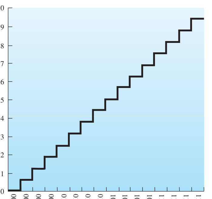
Vout = - aVref *Bin 8b The analog output voltages for our 4-bit converter are given in Figure 15–6(b).
Digital input (b)
Figure 15–6 (Continued ) (b) Analog output versus digital input.
15–4. If the first three resistors in a binary-weighted D/A converter are 30,
60, and 120k�, the fourth resistor, used for the D0 input, must be 15–5. Why is it difficult to build an accurate 8-bit binary-weighted D/A converter? 15–6. To build an 8-bit R/2R ladder D/A converter, you would need at least eight different resistor sizes. True or false? 15–7. If Vref is changed to 6 V in the R/2R converter of Figure 15–6(a), the maximum value at Vout will be 11.25 V. True or false?
15–5 Integrated-Circuit D/A Converters
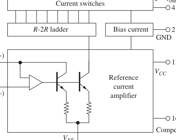
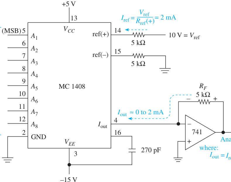
One very popular and inexpensive 8-bit D/A converter (DAC) is the DAC0808 and its equivalent, the MC1408. A block diagram, pin configuration, and typical application are shown in Figure 15–7. The circuit in Figure 15–7(c) is set up to accept an 8-bit dig-
| ital input and provide a 0- to | +10@V | analog output. A reference current (Iref) is required |
|---|---|---|
| for the D/A and is provided by the 10-V, | 5@k� | combination shown. The negative ref- |
| erence (pin 15) is then tied to ground via an equal-size | (5@k�) | resistor. A compensa- |
tion capacitor is connected from pin 16 to 3 to eliminate noise in the output. The 2-mA reference current dictates the full-scale output current (Iout) to also be approximately 2 mA. To calculate the actual output current, use the following formula:
Iout = Iref * aA1 2+ A2 4+ ... + A8 256b
[For example, with all inputs (A1 to A8) HIGH, Iout = Iref * (255/256).] To convert an
| MSB | LSB | ||||||
|---|---|---|---|---|---|---|---|
| A1 | A2 | A3 | A4 | A5 | A6 | A7 | A8 |
| NC | 1 | 16 | Compen. | ||||
| 5 | 6 | 7 | 8 | 9 | 10 | 11 | 12 |
Iout
Current switches GND 2 15 Vref (–)
Top view NPN current source pair
| (a) | (b) |
|---|---|
| Figure 15–7 | The MC 1408 D/A converter: (a) block diagram; (b) pin configuration; |
(c)
Figure 15–7 (Continued ) (c) typical application.
ground and the output taken across the resistor. This method is simple, but it may cause inaccuracies as various-size loads are connected to it. A more accurate method uses an op amp such as the 741 shown in Figure
| 15–7(c). The output current flows through | RF, | which develops an output voltage equal | |||
|---|---|---|---|---|---|
| Team | to Discussion | Iout * RF. ited only by the specifications of the op amp used. | The range of output voltage can be changed by changing | RF | and is lim- |
To test the circuit, an oscillator and an 8-bit counter can be used to drive the digHow could the D/A ital inputs, and the analog output can be observed on an oscilloscope, as shown in converter be driven to
| create a triangle | Figure 15–8. In Figure 15–8, as the counters count from 0000 0000 up to 1111 1111, | |
|---|---|---|
| the analog output will go from 0 V up to almost | +10V | in 256 values. The time per step |
waveform? A square
wave? will be equal to the reciprocal of the input clock frequency. 1
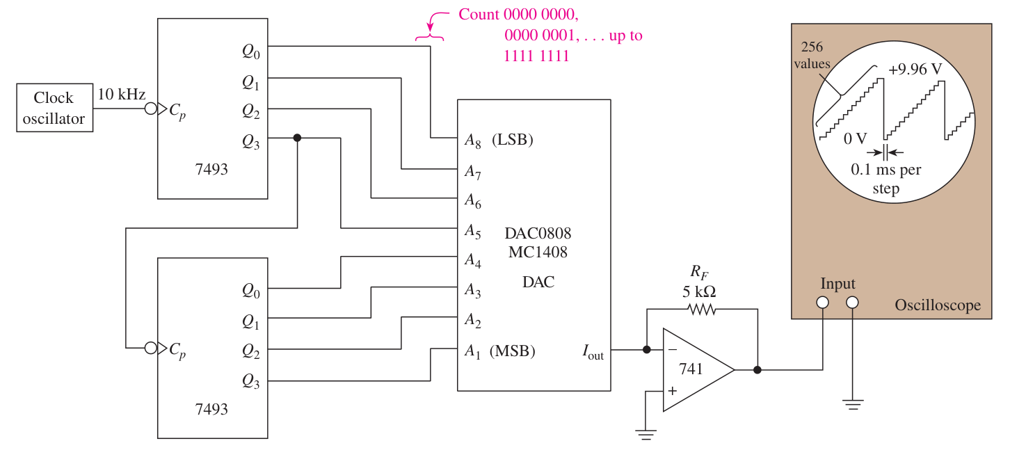
Figure 15–8 Using an 8-bit counter to test the 256-step output of a DAC.
Figure 15–9 shows a MultiSIM®simulation of an 8-bit digital-to-analog
converter. The Word Generator (XWG1) is set up to count 0 through F16
(00002-11112). These digital values are converted to an analog voltage MultiSIM Exercise: Load the file fig15_9 from the textbook companion website. Double-click the oscilloscope to expand its size, and then turn on the power switch. Turn off the power after the single sweep is complete. Count the number of steps for each cycle (should be 16). Drag vertical cur-
sors #1 and #2 to measure the time period of one step (should be 100ms). two steps (should be 19.5 mV). XWG1
16 0 O O O X X X X
| 31 | 15 |
|---|---|
| T | R |
MOD-16 counter Digital input VCC
| 5 V | Analog |
|---|---|
| Vref | D0 D1 D2 D3 D4 D5 D6 D7 |
| + | output |
VDAC − G
| XSC1 | T | |
|---|---|---|
| A | B | |
| fig15_9 | fig15_9 | fig15_9 |
| Figure 15–9 | Using MultiSIM®to simulate the waveforms of a DAC driven by |
a MOD-16 counter.
EXAMPLE 15–3
Determine Iout and Vout in Figure 15–7(c) if the following binary strings are
(a) Using Equation 15–2,
| Iout = Iref * aA1 | 2+ A2 | 4+ c + A8 | 256b | |||||
|---|---|---|---|---|---|---|---|---|
| = 2mA * a1 | 2+ 1 | 4+ 1 64+ = 2mA * a255 | 8+ 1 128+ 256b | 16+ 1 | 32+ 1 | 1 | 256b | 1 |
= 1.99mA
and Vout = Iout * RF = 9.96V (b) Using Equation 15–2,
| Iout = Iref * aA1 | 2+ A2 | 4+ c + A8 | 256b | ||
|---|---|---|---|---|---|
| = 2mA * a1 | 2+ 1 | 16+ 1 32+ = 2mA * a155 | 1 128+ 256b | 256b | 1 |
= 1.21mA
and Vout = Iout * RF = 6.05V There are two ways to arrive at the fraction 155/256 in the above solution. One way is to find a common denominator for all the fractions and then add them together, as we did. The other way is to convert the binary input 1001 1011 into decimal, which equals 155, and then divide that by 256. The new equation becomes the following:
Iout = Iref * aBinaryinput10 b 25610
15–6 Integrated-Circuit Data
Converter Specifications
In addition to resolution, several other specifications are important in the selection of D/A and analog-to-digital (A/D) converters (DACs and ADCs). It is important that the specifications and their definitions given in the manufacturer’s data book be studied and understood before selecting a particular DAC or ADC. Figure 15–10 lists some of the more important specifications as presented in the Signetics Linear LSI Data Manual.
| 111 | High gain | Ideal | 111 | ||||||
|---|---|---|---|---|---|---|---|---|---|
| 110 | 110 | ||||||||
| Digital output | 101 Analog output Step size error Differential nonlinearity | Digital output 100 011 010 001 000 | 101 100 Low gain 010 001 000 | ||||||
| 0 | 0 | 0 | 0 | 1 | 1 | 1 | 1 | ||
| 0 | 0 | 1 | 1 | 0 | 0 | 1 | 1 | Analog input | Analog input |
| 0 | 1 | 0 Digital input | 1 (c) | 0 | 1 | 0 | 1 | (b) | (Shows a missing code at 101) |
(a) Ideal 1/2 LSB diff. nonlinear
| 111 | 111 | Nonideal | ||||
|---|---|---|---|---|---|---|
| 1 | Offset | |||||
| Analog output | 1 | Digital output | 110 | error | Digital output | 110 |
| 1 | 2 | FS-LSB | ||||
| 1 | LSB | 101 | Perfect | 101 | ||
| LSB | 1/2 LSB | 100 | ADC | 100 | ||
| 1 | 011 1 | 011 LSB diff. | ||||
| 2 | ADC with offset 001 000 | 010 001 000 | ||||
| 000 | 010 | 100 | 110 | |||
| 001 | 011 | 101 | 111 | Analog input | 1/2 LSB | Analog input |
| Digital input | (e) | (f) |
(d) E0 Ideal transfer function
| ±1/2 | Digital output | 110 |
|---|---|---|
| LSB | 101 t 0 | 000 Settling |
Analog input time
| (g) | (h) | |
|---|---|---|
| Figure 15–10 | DAC and ADC specification definition: (a) differential nonlinearity; (b) gain | |
| error; (c) missing codes; (d) nonmonotonic (must be | 7;1 | LSB nonlinear); (e) offset error; |
(f) relative accuracy; (g) settling time; (h) 3-bit ADC transfer characteristic. (Used with permission from NXP Semiconductors.)
Review Questions
15–8. Is the analog output of the MC1408 DAC IC represented by current or voltage? 15–9. Which digital input to the MC1408 DAC IC has the most significant effect on the analog output: A1, or A8?
15–11. A DAC is nonmonotonic if its analog output drops after a 1-bit
increase in digital input. True or false? 15–12. Which error affects the rate of change, or slope, of the ideal transfer function of an ADC, the gain error or the offset error?
15–7 Parallel-Encoded A/D Converters
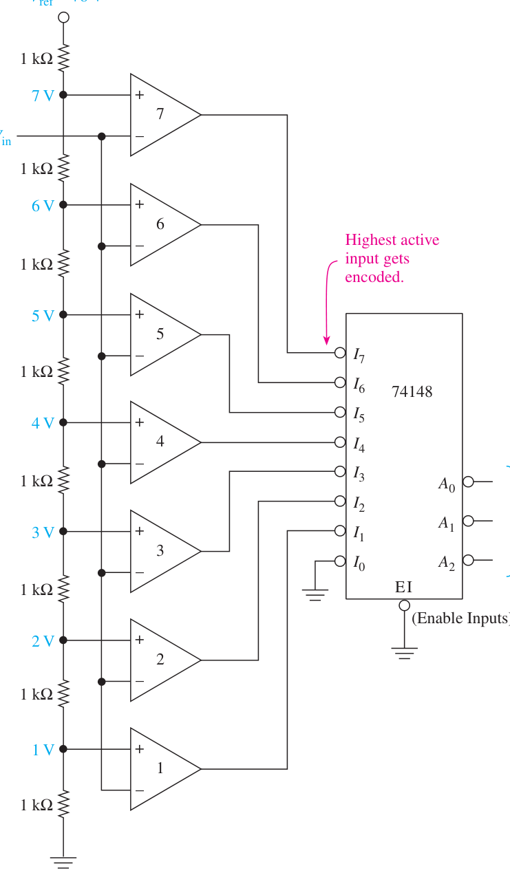
The process of taking an analog voltage and converting it to a digital signal can be done in several ways. One simple way that is easy to visualize is by means of parallel encoding (also known as simultaneous, multiple comparator, or flash converting). In this method, several comparators are set up, each at a different voltage reference level with their outputs driving a priority encoder, as shown in Figure 15–11. The voltage-divider Vref = +8 V
(b)
Figure 15–11 Three-bit parallel-encoded ADC: (a) block diagram and (b) circuit diagram.
voltage reference at each comparator input in 1-V steps.
| When Vin is 0 V, the | (+) | input on all seven comparators will be higher than the | |
|---|---|---|---|
| (-) | input, so they will all output a HIGH. In this case, | I0 | is the only active-LOW input |
that is enabled, so the 74148 will output an active-LOW binary 0 (111).
When Vin exceeds 1.0 V, comparator 1 will output a LOW. Now I0 and I1 are both increases further, each successive comparator outputs a LOW. The highest input that receives a LOW is encoded into its binary equivalent output. The A/D converter in Figure 15–11 is set up to convert analog voltages in the range from 0 to 7 V. The range can be scaled higher or lower, depending on the input voltage levels that are expected. The resolution of this converter is only 3 bits, so it can only distinguish among eight different analog input levels. To expand to 4-bit resolution, eight more comparators are required to differentiate the 16 different voltage levels. To expand to 8-bit resolution, 256 comparators would be required! As you can see, circuit complexity becomes a real problem when using parallel encoding for highresolution conversion. However, a big advantage of using parallel encoding is its high speed. The conversion speed is limited only by the propagation delays of the comparators and encoder (less than 20 ns total). Helpful
15–8 Counter-Ramp A/D Converters
Hint This circuit is made The counter-ramp method of A/D conversion (ADC) uses a counter in conjunction completely of devices that with a D/A converter (DAC) to determine a digital output that is equivalent to the unhave already been known analog input voltage. In Figure 15–12, depressing the start conversion push butdiscussed, which makes it
ton clears the counter outputs to 0, which sets the DAC output to 0 V. The (-) input to
| the comparator is now 0 V, which is less than the positive analog input voltage at the | timing and interface |
|---|---|
| (+) | input. Therefore, the comparator outputs a HIGH, which enables the AND gate, |
between multiple ICs.
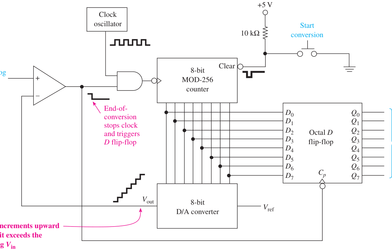
Figure 15–12 Counter-ramp A/D converter.
does the DAC output voltage in the form of a staircase. When the staircase voltage reaches and then exceeds the analog input voltage, the comparator output goes LOW, disabling the clock and stopping the counter. The counter output at that point is equal to the binary number that caused the DAC to output a voltage slightly greater than the analog input voltage. Thus, we have the binary equivalent of the analog voltage! The HIGH-to-LOW transition of the comparator is also used to trigger the D flipflop to latch on to the binary number at that instant. To perform another conversion, the start push button is depressed again, and the process repeats. The result from the previous conversion remains in the D flip-flop until the next end-of-conversion HIGHto-LOW edge comes along. To change the circuit to perform continuous conversions, the end-of-conversion line could be tied back to the clear input of the counter. A short delay needs to be inserted into this new line, however, to allow the D flip-flop to read the binary number before the counter is Reset. Two inverters placed end to end in the line will produce a sufficient delay. The main disadvantage of the counter-ramp method of conversion is its slow conversion speed. The worst-case maximum conversion time will occur when the
counter has to count all 255 steps before the DAC output voltage matches the analog [tmax = 256 * (1>fcp)].
Review Questions
15–13. In the parallel-encoded ADC of Figure 15–11, only one of the
comparators will output a LOW for each analog input value. True or false? 15–14. One difficulty in building a high-resolution, 10-bit, parallelencoded ADC is that it would take _________ comparators to complete the design. 15–15. The counter-ramp ADC of Figure 15–12 signifies an “end of con-
version” when the (-) input voltage to the comparator drops below the (+) 15–16. The digital output of the octal D flip-flop in Figure 15–12 is continuously changing at the same rate as the MOD-256 counter. True or false?
15–9 Successive-Approximation A/D Conversion
Other methods of A/D conversion employ up/down-counters and integrating slope converters to track the analog input, but the method used in most modern IC ADCs is called successive approximation. This converter circuit is similar to the counterramp ADC circuit, except that the method of narrowing in on the unknown analog input voltage is much improved. Instead of counting up from 0 and comparing the DAC output each step of the way, a successive-approximation register (SAR) is used in place of the counter (see Figure 15–13).
| In Figure 15–13, the conversion is started by dropping the | STRT | line LOW. Then |
|---|---|---|
| Team | the SAR first tries a HIGH on the MSB (D7) line to the DAC. (Remember, D7 will Discussion | cause the DAC to output half of its full-scale output.) If the DAC output is then higher |
than the unknown analog input voltage, the SAR returns the MSB LOW. If the DAC Why is the SAR converter
| much faster than the | output was still lower than the unknown analog input voltage, the SAR leaves the MSB |
|---|---|
| counter-ramp? | HIGH. |
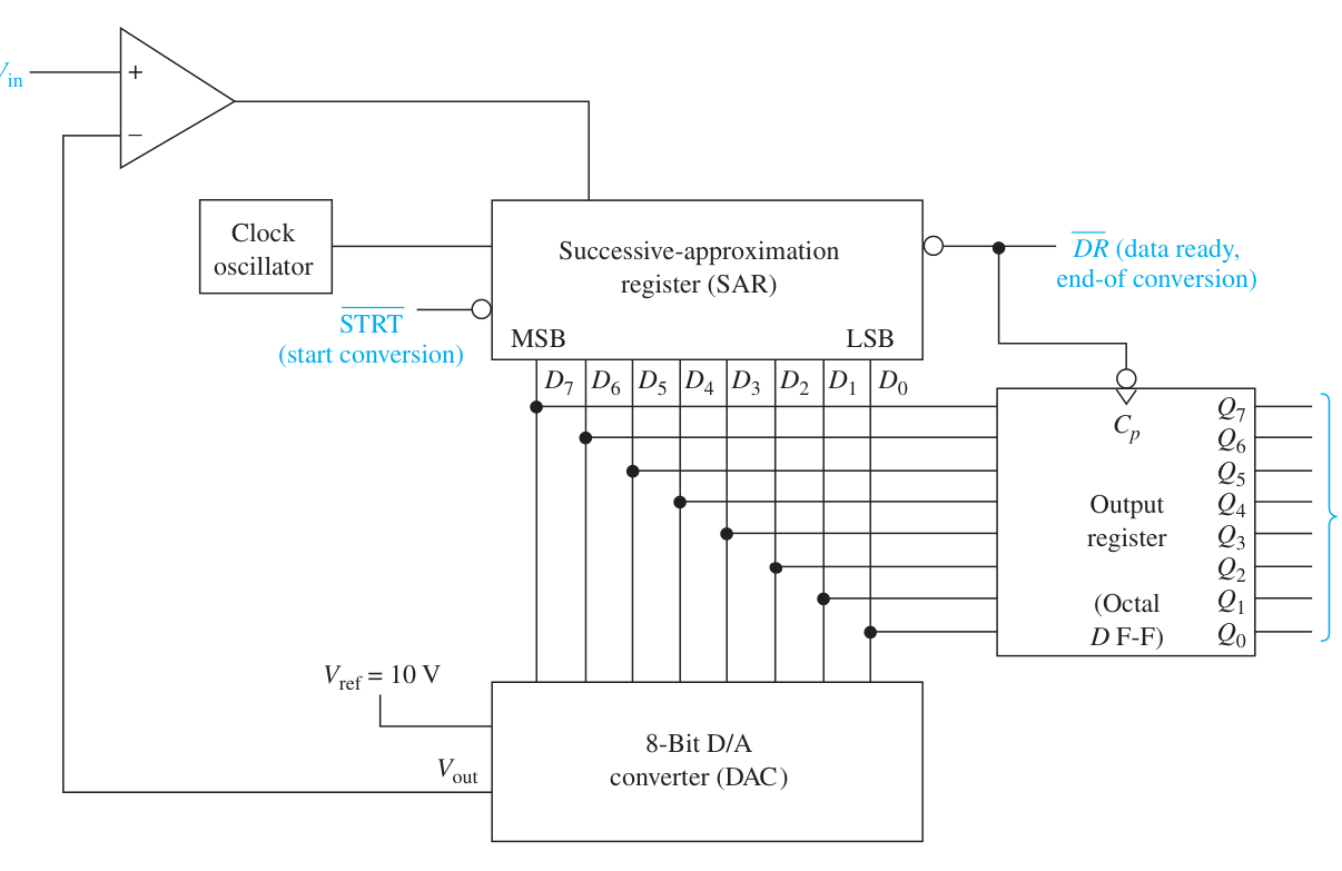
Figure 15–13 Simplified SAR A/D converter.
Now, the next lower bit (D6) is tried. If a HIGH on D6 causes the DAC output to be higher than the analog Vin, it is returned LOW. If not, it is left HIGH. The process continues until all 8 bits, down to the LSB, have been tried. At the end of this eightstep conversion process, the SAR contains a valid 8-bit binary output code that repre-
| sents the unknown analog input. The | DR | output now goes LOW, indicating that the |
|---|---|---|
| conversion is complete and the data are ready. The HIGH-to-LOW edge on | DR | clocks |
the D0 to D7 data into the octal D flip-flop to make the digital output results available
at the Q0 to Q7 lines.
Figure 5–13 takes only eight clock periods to complete a conversion, which is a vast [tmax = 8 * (1>fcp)].
improvement over the counter-ramp method Notice that with the where as with the counter-ramp, it is slightly more.
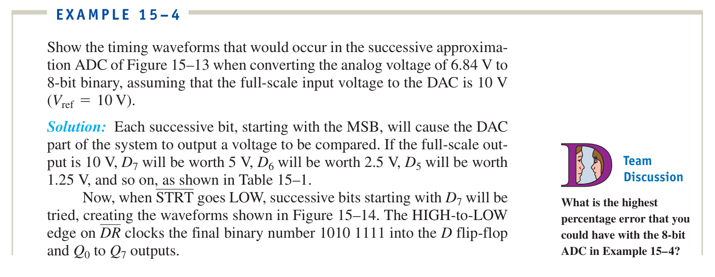
by Each Successive Approximation Register Bit
| DAC Input | DAC Vout |
|---|---|
| D7 | 5.0000 |
| D6 | 2.5000 |
| D5 | 1.2500 |
| D4 | 0.6250 |
| D3 | 0.3125 |
| D2 | 0.15625 |
| D1 | 0.078125 |
| D0 | 0.0390625 |
10 μs 100 kHz clock
STRT Start conversion Data ready DR
| D7 | 1 |
|---|---|
| D6 | 0 |
| D5 | 1 |
| D4 | 0 |
| D3 | 1 |
| D2 | 1 |
| D1 | 1 |
| D0 | 1 |
Final digital output
| 8 | 7.50000 | |
|---|---|---|
| 6.8750 | 6.5625 6.71875 | 6.8359375 |
| 7 | 6.2500 |
DAC Vout
| 6 | 5.0000 | 6.796875 |
|---|---|---|
| 1 | 0.00 |
Conversion time = 80 μs
Figure 15–14 Timing waveforms for a successive approximation A/D conversion.
Now the Q0 to Q7 lines contain the 8-bit binary representation of the analog number 6.8359375, which is an error of only 0.0594% from the target number of 6.84: %error =actualvoltage - finalDACoutput
* 100% (15–4)
logic analyzer can be connected to the D0 to D7 outputs of the SAR.
| For continuous conversions, the | DR | line can be connected back to the | ||
|---|---|---|---|---|
| STRT | line. That way, as soon as the conversion is complete, the HIGH-to- | |||
| LOW on | DR | will issue another start conversion | (STRT), | which forces the |
| data ready | (DR) | line back HIGH for eight clock periods while the new |
conversion is being made. The latched Q0 to Q7 digital outputs will always display the results of the previous conversion.
15–10 Integrated-Circuit A/D Converters
Examples of two popular, commercially available ADCs are the NE5034 and the ADC0804 manufactured by NXP Semiconductors.
The NE5034
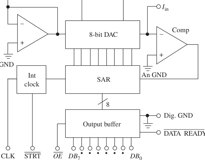
The block diagram and pin configuration for the NE5034 are given in Figure 15–15. Operation of the NE5034 is almost identical to that of the SAR ADC presented in Section 15–9. One difference is that the NE5034 uses a three-state output buffer in-
stead of a D flip-flop. With three-state outputs, when OE (Output Enable) is LOW, the
OE line goes HIGH, the DB7 to DB0 outputs return to a float or high-impedance state. DB7 to DB0 float, one of the other devices can output information to the data bus without interference.
The NE5034 can provide conversion speeds as high as one per 17ms, and its also has its own internal clock for providing timing pulses. The frequency is determined by an external capacitor placed between pins 11 and 17. Figure 15–16 shows the frequency and conversion time that can be achieved using the internal clock.
Iref in +VCC –VCC
(MSB) (MSB)
Figure 15–15 The NE5034 A/D converter: (a) block diagram and (b) pin configuration.
(Used with permission from NXP Semiconductors.)
Conversion Time (μ sec)
10,000 40
| 1000 | 30 | ||||||||
|---|---|---|---|---|---|---|---|---|---|
| 100 | 20 | ||||||||
| 10 | 10 | ||||||||
| 1 | 0 | ||||||||
| 1 | 10 | 100 | 1000 10,000 100,000 | 300 | 400 | 500 | 600 | 700 | 800 |
| Capacitor (CL) in pF | Frequency (KHz) | ||||||||
| (a) | (b) | ||||||||
| Figure 15–16 | The NE5034 internal clock characteristics: (a) internal clock frequency |
versus external capacitor (CL) and (b) conversion time versus clock frequency. (Used with permission from NXP Semiconductors.)
The ADC0804
The pin configuration and block diagram for the ADC0804 are given in Figure 15–17. The ADC0804 uses the successive-approximation method to convert an analog input to an 8-bit binary code. Two analog inputs are provided to allow differential measure-
| ments [analog | Vin = Vin(+) - Vin(-) | ]. It has an internal clock that generates its own |
|---|---|---|
| timing pulses at a frequency equal to | f = 1/(1.1RC) | (Figure 15–18 shows the connec- |
tions for the external R and C). It uses output D latches that are three-stated and
controlled by RD to facilitate easy bus interfacing. (See Figure 15–23 for interfacing to The convention for naming the ADC0804 pins follows that used by microprocessors to ease interfacing. Basically, the operation of the ADC0804 is similar to that of the NE5034. The ADC0804 pins are defined as follows:
| CS | —active-LOW Chip Select |
|---|---|
| RD | —active-LOW Output Enable |
| WR | —active-LOW Start Conversion |
CLK IN—external clock input or capacitor connection point for the internal clock
| INTR | —active-LOW End-of-Conversion (Data Ready) | |
|---|---|---|
| Vin(+), | Vin(-) | —differential analog inputs (ground one pin for single-ended |
measurements)
Vref/2—optional reference voltage (used to override the reference voltage
assumed at VCC) VCC—5-V power supply and assumed reference voltage CLK R—resistor connection for the internal clock D0 to D7—digital outputs To set the ADC0804 up for continuous A/D conversions, the connections shown in Figure 15–18 should be made. The external RC will set up a clock frequency of
| 1 | 1 | |||
|---|---|---|---|---|
| f = | 1.1RC= | 1.1(10k�)150pF= 606kHz | (15–5) | |
| The connection from | INTR | to | WR | will cause the ADC to start a new conversion |
| each time the | INTR | (end-of-conversion) line goes LOW. The RC circuit with the |
| 6 | 7 |
|---|---|
| + | − |
| 9 | + |
| Vref/2 | Auto zero |
Ladder and
| 8 | decoder | comparator |
|---|---|---|
| GNDA | – |
D7
| (MSB) | 11 |
|---|---|
| 20 | D6 |
| +5 V VCC | 12 |
D5 D4
| Output | 14 | |
|---|---|---|
| latches | D3 | 15 |
| D2 | 16 | |
| SAR | D1 | |
| 10 | D0 | |
| (LSB) | 18 |
GNDD
LE OE
WR 8-bit shift register CS
S Intr.
2 R Q
| CLK in | CLK R | |
|---|---|---|
| 5 | 4 | 19 |
INTR 150 pF 10 K (a)
| CS | 1 | 20 | VCC |
|---|---|---|---|
| RD | 2 | 19 | CLK R |
| WR | 3 | 18 | D0 |
| CLK in | 4 | 17 | D1 |
| INTR | 5 | 16 | D2 |
| Vin(+) | 6 | 15 | D3 |
| Vin(–) | 7 | 14 | D4 |
| A GND | 8 | 13 | D5 |
| Vref/2 | 9 | 12 | D6 |
| D GND | 10 | 11 | D7 |
(b)
Figure 15–17 The ADC0804 converter: (a) block diagram and (b) pin configuration.
(Used with permission from NXP Semiconductors.) 7417 open-collector buffer will issue a LOW-to-float pulse at power-up to ensure initial startup. An open-collector output gate is required instead of a totem-pole output
because the INTR is forced LOW by the internal circuitry of the 0804 at the end of each
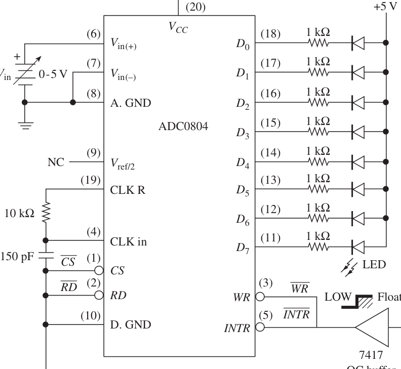
Figure 15–18 Connections for continuous conversions using the ADC0804.
were used. The CS is grounded to enable the ADC chip. RD is grounded to enable the
| Vin(+). | If it were negative, | Vin(+) | would be grounded, and the input voltage would be | |
|---|---|---|---|---|
| connected to | Vin(-). | Differential measurements (the difference between two analog | ||
| voltages) can be made by using both | Vin(+) | and | Vin(-). | The LEDs connected to the dig- |
ital output will monitor the operation of the ADC outputs. An LED ON indicates a LOW, and an LED OFF indicates a HIGH. (In other words, they are displaying the complement of the binary output.) To test the circuit operation, you could watch the OFF LEDs count up in binary from 0 to 255 as the analog input voltage is slowly in-
creased from 0 to +5V. (In other words, you could watch the ON LEDs count down.) using the Vref/2 input. This provides the means of encoding small analog voltages to the full 8 bits of resolution. The Vref/2 pin is normally not connected, and it sits at 2.500 V (VCC/2). By connecting 2.00 V to Vref/2, the analog input voltage range is changed to 0 through 4 V; 1.5 V would change it to 0 through 3.0 V and so on. However, the accuracy of the ADC suffers as the input voltage range is decreased. Because the analog input voltage is directly proportional to the digital output, the following ratio can be used as an equation to solve for the digital output value:
Ain =Dout
Vref 256 Dout =Ain
* 256 (15–7) whereAin = analoginputvoltage
| Vref = reference | voltage (Vpin20 or | Vpin9 * 2) |
|---|---|---|
| Dout = digital | output (converted to base 10) 256 = total | number of digital output steps (0 to 255, inclusive) |
provided to enhance the accuracy of the system. The VCC -to-digital ground lines are inlog and digital grounds is not mandatory, but when used, they ensure that the analog voltage comparator will not switch falsely due to digital noise and jitter.
EXAMPLE 15–5
Change VCC (pin 20) in Figure 15–18 to 5.12 V. Determine which LEDs (a) 5.100 V; (b) 2.26 V.
Solution:
Dout =Ain
(a) * 256 =5.100V 5.120V* 256 = 25510 = 111111112 Because the LEDs are active-LOW, none of them will be ON. Dout =Ain
(b) * 256 =2.26V 5.12V* 256 = 11310 = 011100012 The following LEDs will be ON: LED7, LED3, LED2, LED1.
ADC SIMULATION
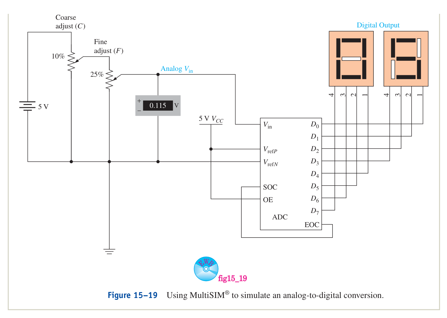
Figure 15–19 shows a MultiSIM®simulation of an 8-bit analog-to-digital
converter. Two potentiometers are used to provide a coarse and a fine adjustment to the analog voltage that is input to the ADC. In this illustration, the analog input voltage is 0.115 V, which is converted to the hex number 05 (0000 01012). The ADC is set up to perform continuous conversions by connecting EOC to SOC as shown. MultiSIM Exercise: Load the file fig15_19 from the textbook companion website. Turn on the power switch and repeatedly press F or shift-F to raise and lower the analog Vin. (a) Determine the average voltage required to make a one bit change in the digital output. (It should be about 20 mV.) (b) Determine the analog Vin required to reach full-scale digital output (FF16). (It should be 5.0 V.)
Review Questions
15–17. The SAR ADC in Figure 15–13 starts making a conversion when
_________ goes LOW and signifies that the conversion is complete when _________ goes LOW. 15–18. The SAR method of A/D conversion is faster than the counter/ ramp method because the SAR clock oscillator operates at a higher speed. True or false? 15–19. Decide if the following pins on the ADC0801 are for input or output signals.
| (a) | CS | (c) | WR |
|---|---|---|---|
| (b) | RD | (d) | INTR |
15–20. List the order in which the signals listed in Question 15–19 become active to perform an A/D conversion.
15–11 Data Acquisition System Application
The computerized acquisition of analog quantities is becoming more important than ever in today’s automated world. Computer systems are capable of scanning several analog inputs on a particular schedule and sequence to monitor critical quantities and acquire data for future recall. A typical eight-channel computerized data acquisition system (DAS) is shown in Figure 15–20.
V0 Temperature Analog
| V1 | multiplexer |
|---|---|
| Pressure | switch |
AM3705 V2
| Displacement | Programmable-gain |
|---|---|
| Sample-and-hold | instrumentation |
| circuit | amplifier |
V3
Velocity Vin Vin
| Inputs | Adjusted | |||
|---|---|---|---|---|
| V4 | LF198 | Vout | LH0084 | Vout |
| Fluid level | C | G0 | ||
| T | G1 | Gain | ||
| V5 | Hold | select |
C
| Kilowatts | capacitor |
|---|---|
| V6 | trigger |
| Humidity | 1-of-8 |
select
Solar V7
Control bus To other
| CS | RD2/WR2 | ||
|---|---|---|---|
| CS1 | RD1 | WR1 | INTR |
| Analog | RAM | ||
| Vin | (memory) |
CLK in
| 8-Bit | Microcontroller |
|---|---|
| A/D converter | data |
| D0 | bus |
| ••• | P |
| ADC0804 | D0 |
O
••• R T
D7 0 To other devices Team
Figure 15–20 Data acquisition system. Discussion
Discuss the flow of a signal as it travels from the temperature transducer through each of the ICs to the microcontroller.
data bus and the control bus. The data bus is simply a common set of eight electrical conductors shared by as many devices as necessary to send and receive 8 bits of parallel data to and from anywhere in the system. In this case, there are three devices on the data bus: the ADC, the microprocessor (or microcontroller), and memory. The control bus passes control signals to and from the various devices for such things as chip select
(CS), output enable (RD), system clock, triggers, and selects. the analog quantity being measured. The task of the microprocessor is to scan all the quantities at some precise interval and store the digital results in memory for future use. Because the analog values vary so slowly, scanning (reading) the variables at 1-s intervals is usually fast enough to get a very accurate picture of their levels. This can easily be accomplished by microprocessors with clock rates in the microsecond range. To do this, the microprocessor must enable and send the proper control signals to each of the devices, in order, starting with the multiplexer and ending with the ADC. This is called handshaking, or polling, and is all done with software statements. If you are fortunate enough to take a course in microprocessor programming, you will learn how to perform some of these tasks. All the hardware interfacing and handshaking that takes place between the microprocessor and the transducers can be explained by taking a closer look at each of the devices in the system.
Analog Multiplexer Switch (AM3705)
The multiplexer reduces circuit complexity and eliminates duplication of circuitry by allowing each of the eight transducer outputs to take turns traveling through the other devices. The microprocessor selects each of the transducers at the appropriate time by setting up the appropriate binary select code on the A, B, and C inputs via the control bus. This allows the selected transducer signal to pass through to the next device.
Sample-and-Hold Circuit (LF198)
Because analog quantities can be constantly varying, it is important to be able to select a precise time to take the measurement. The sample-and-hold circuit, with its external Hold capacitor, allows the system to take (Sample) and Hold an analog value at the precise instant that the microprocessor issues the acquisition trigger.
Programmable-Gain Instrumentation Amplifier (LH0084)
Each of the eight transducers has different full-scale output ratings. For instance, the temperature transducer may output in the range from 0 to 5 V, whereas the pressure transducer may only output 0 to 500 mV. The LH0084 is a programmable-gain amplifier capable of being programmed, via the gain select inputs, for gains of 1, 2, 5, or 10. When it is time to read the pressure transducer, the microprocessor will program the gain for 10 so that the range will be 0 to 5 V, to match that of the other transducers. This way, the ADC can always operate in its most accurate range, 0 to 5 V.
Analog-to-Digital Converter (ADC0804)
The ADC receives the adjusted analog voltage and converts it to an equivalent 8-bit bi-
| nary string. To do this, the microprocessor issues chip select | (CS1) | and start conversion | |
|---|---|---|---|
| (WR1) | pulses. When the end-of-conversion | (INTR) | line goes LOW, the microprocessor |
| issues an output enable | (RD1) | to read the data (D0 and D7) that pass, via the data bus, |
into the microprocessor and then into the random-access memory (RAM) chip (more on memory in Chapter 16).
mines that it is time for the next scan. Other software routines executed by the microprocessor will act on the data that have been gathered. Some possible responses to the measured results might be to sound an alarm, speed up a fan, reduce energy consumption, increase a fluid level, or simply produce a tabular report of the measured quantities.
15–12 Transducers and Signal Conditioning
Hundreds of transducers are available today that convert physical quantities such as heat, light, or force into electrical quantities (or vice versa). The electrical quantities (or signal levels) must then be conditioned (or modified) before they can be interpreted by a digital computer. Signal conditioning is required because transducers each output different ranges and types of electrical signals. For example, transducers can produce output voltages or output currents or act like variable resistances. A transducer may have a nonlinear response to input quantities, may be inversely proportional, and may output signals in the microvolt range. A transducer’s response specifications are given by the manufacturer and must be studied carefully to determine the appropriate analog signal-conditioning circuitry required to interface it to an A/D converter. After the information is read into a digital computer, software instructions convert the binary input into a meaningful output that can be used for further processing. Let’s take a closer look at three commonly used transducers: a thermistor, an IC temperature sensor, and a strain gage.
Thermistors
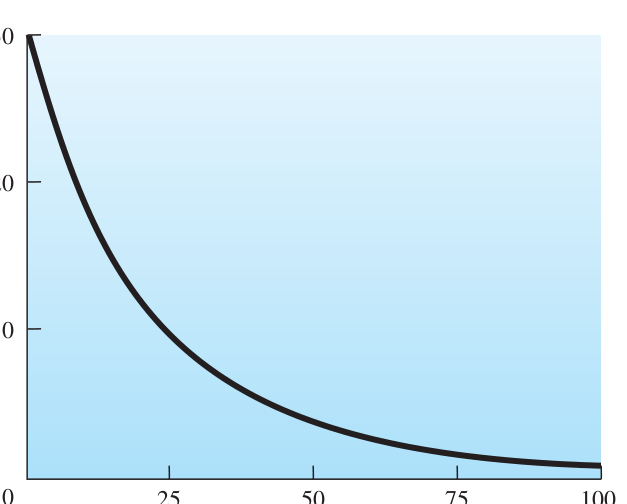
A thermistor is an electronic component whose resistance is highly dependent on temperature. Its resistance changes by several percent with each degree change in temperature. It is a very sensitive temperature-measuring device. One problem, however, is
that its response is nonlinear, meaning that 1� step changes in temperature will not cre-
of the 10@k� (at 25�C) thermistor shown in Figure 15–21.
Temperature (°C)
Figure 15–21 Thermistor characteristic curve of resistance versus temperature.
From the characteristic curve, you can see that not only is this thermistor nonlinear, but it also has a negative temperature coefficient (i.e., its resistance decreases with increasing temperatures).
mistor resistance to a voltage in the range of 0 to 5 V. One way to accomplish this task is with the circuit shown in Figure 15–22. –10 V 200 kΩ 390 Ω Rf
| –250 mV | – | |
|---|---|---|
| 10 kΩ | RT | Rf |
Vout = – (–250 mV) ×
| + | Ri | |
|---|---|---|
| 10 Ω | Ri | (To Vin of an ADC) |
| Figure 15–22 | Circuit used to convert thermistor ohms to a dc voltage. |
This circuit operates similarly to the op-amp circuit explained in Section 15–2. The output of the circuit is found using the formula Rf
Vout = -Vin * (15–8)
Ri
| where Vin is a fixed reference voltage of | -250 | mV and Ri is the sum of the thermistor’s |
|---|---|---|
| resistance, RT, plus | 10k�. | Using specific values for RT found in the manufacturer’s |
data manual, we can create Table 15–2, which shows Vout as a function of temperature.
TABLE 15–2 Tabulation of Output Voltage Levels for a Temperature
| Temperature | RT | Ri | Vout | ||||
|---|---|---|---|---|---|---|---|
| (in �C) | (in k | � | ) | (in k | � | ) | (in V) |
| 0 | 29.490 | 39.490 | 1.27 | ||||
| 25 | 10.000 | 20.000 | 2.50 | ||||
| 50 | 3.893 | 13.893 | 3.60 | ||||
| 75 | 1.700 | 11.700 | 4.27 | ||||
| 100 | 0.817 | 10.817 | 4.62 |
The output voltage, Vout, is fed into an ADC that converts it into an 8-bit binary number. The binary number is then read by a microprocessor that converts it into the corresponding degrees Celsius using software program instructions.
Linear IC Temperature Sensors
The computer software required to convert the output voltages of the previous thermistor circuit is fairly complicated because of the nonlinear characteristics of the device. Linear temperature sensors were developed to simplify the procedure. One such device is the LM35 IC temperature sensor. It is fabricated in a three-terminal transistor package and is designed to output 10 mV for each degree Celsius above zero. (Another temperature sensor, the LM34, is calibrated in degrees Fahrenheit.) For example, at
25�C the sensor outputs 250 mV, at 50�C it outputs 500 mV, and so on, in linear steps and microprocessor.
+5 V temperature
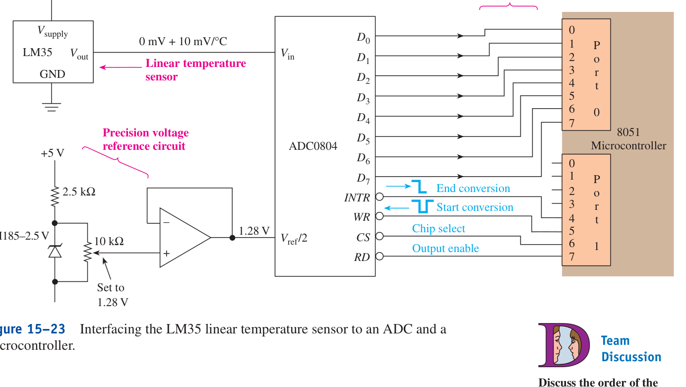
| The 1.28-V reference level used in Figure 15–23 is the key to keeping the con- | control signals between | |
|---|---|---|
| version software programming simple. With 1.28 V at Vref/2, the maximum full-scale | the microcontroller and | |
| analog Vin is defined as 2.56 V (2560 mV). This value corresponds one-for-one with | the ADC. | |
| the 256 binary output steps provided by an 8-bit ADC. A | 1� | rise in temperature in- |
creases Vin by 10 mV, which increases the binary output by 1. Therefore, if Vin equals 0 V, D7 to D0 equals 0000 0000; if Vin equals 2.55 V, D7 to D0 equals 1111 1111; and if Vin equals 1.00 V, D7 to D0 equals the binary equivalent of 100, which is 0110 0100.
Table 15–3 lists some representative values of temperature versus binary output.
TABLE 15–3 Tabulation of Temperature versus Binary and an ADC Set Up for 2560 mV Full Scale
| Temperature | Vin | Binary Output |
|---|---|---|
| (in �C) | (in mV) | (D7 to D0) |
| 0 | 0 | 0000 0000 |
| 1 | 10 | 0000 0001 |
| 2 | 20 | 0000 0010 |
| 25 | 250 | 0001 1001 |
| 50 | 500 | 0011 0010 |
| 75 | 750 | 0100 1011 |
| 100 | 1000 | 0110 0100 |
In Figure 15–23, the LM185 is a 2.5-V precision voltage reference diode. This
| diode maintains a steady 2.5 V across the | 10@k� | potentiometer even if the 5-V power |
|---|---|---|
| supply line fluctuates. The | 10@k� | potentiometer must be set to output exactly 1.280 V. |
The op amp is used as a unity-gain buffer between the potentiometer and ADC and will maintain a steady 1.280 V for the Vref/2 pin.
The strain gage is a device whose resistance changes when it is stretched. The gage is stretched, or elongated, when it is “strained” by a physical force. This property makes it useful for measuring weight, pressure, flow, and acceleration. Several types of strain gages exist, the most common being the foil type illustrated in Figure 15–24. The gage is simply a thin electrical conductor that is looped back and forth and bonded securely to the piece of material to be strained (see Figure 15–25). Applying a force to the metal beam bends the beam slightly, which stretches the strain gage in the direction of its sensitivity axis. Sensitivity axis Solder tabs
| (a) | (b) |
|---|---|
| Figure 15–24 | A foil-type strain gage: (a) sketch and (b) photograph. |
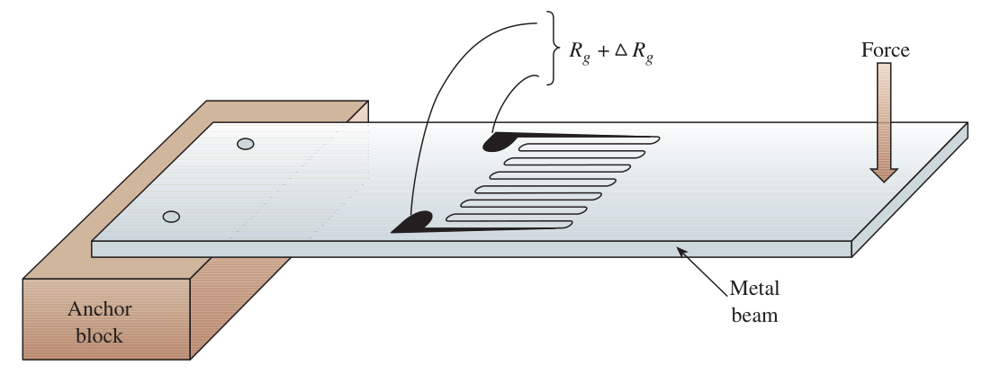
Figure 15–25 Using a strain gage to measure force.
As the strain gage conductor is stretched, its cross-sectional area decreases and its length increases, thus increasing the resistance measured at the solder tabs. The change in resistance is linear with respect to changes in the length of the strain gage. However, the change in resistance is very slight, usually milliohms, and it must be converted to a voltage and amplified before it is input to an ADC. Figure 15–26 shows the
signal conditioning circuitry for a 120@� strain gage [Rg(unstrained) = 120�]. The
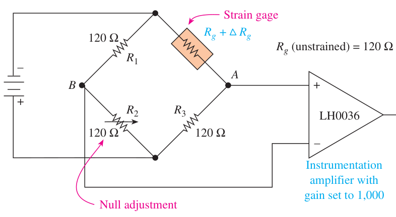
Figure 15–26 Signal conditioning for a strain gage.
instrumentation amplifier is a special-purpose IC used to amplify small-signal differential voltages such as those at points A and B in the bridge circuit in Figure 15–25.
With the metal beam unstrained (no force applied), the 120- � potentiometer is the metal beam, elongating the strain gage and increasing its resistance slightly from
its unstrained value of 120 �. This increase causes the bridge circuit to become voltage is calculated by the following formula:
| VAB = Vinc | R3 | R2 | d |
|---|---|---|---|
| R3 + (Rg + �Rg)- | (15–9) |
R1 + R2
| For example, if R2 is set at | 120� | and | �Rg | is | 150m�, | the voltage is as follows: |
|---|---|---|---|---|---|---|
| VAB = -10c | 120 | 120 + 120d = 3.12mV | 120 |
120 + (120.150)Because the instrumentation amplifier gain is set at 1000, the output voltage sent to the ADC will be 3.12 V. Through experimentation with several known weights, the relationship of force versus Vout can be established and programmed into the microprocessor reading the ADC output.
Review Questions
15–21. The AM7305 multiplexer in Figure 15–20 is used to apply the appropriate voltage gain to each of the transducers connected to it. True or false? 15–22. The 8-bit data out from the ADC in Figure 15–20 passes to the microprocessor via the data bus. True or false? 15–23. Signal conditioning is required to make transducer output levels compatible with ADC input requirements. True or false? 15–24. What is the advantage of using the LM35 linear temperature sensor over a thermistor for measuring temperature?
In this chapter, we have learned the following:
1. Any analog quantity can be represented by a binary number. Longer
binary numbers provide higher resolution, which gives a more accurate representation of the analog quantity.
- 2. Operational amplifiers are important building blocks in analog-to-digital
(A/D) and digital-to-analog (D/A) converters. They provide a means for summing currents at the input and converting a current to a voltage at the output of converter circuits.
- 3. The binary-weighted D/A converter is the simplest to construct, but it
has practical limitations in resolution (number of input bits).
- 4. The R/2R ladder D/A converter uses only two different resistor values,
no matter how many binary input bits are included. This allows for very high resolution and ease of fabrication in IC form.
5. The DAC0808 (or MC1408) IC is an 8-bit D/A converter that uses the
R/2R ladder method of conversion. It accepts 8 binary input bits and outputs an equivalent analog current. Having 8 input bits means that it can resolve up to 256 unique binary values into equivalent analog values.
- 6. Applying an 8-bit counter to the input of an 8-bit D/A converter will
produce a 256-step sawtooth waveform at its output.
- 7. The simplest way to build an analog-to-digital (A/D) converter is to use
the parallel encoding method. The disadvantage is that it is practical only for low-resolution applications.
8. The counter-ramp A/D converter employs a counter, a D/A converter,
and a comparator to make its conversion. The counter counts from zero up to a value that causes the D/A output to exceed the analog input value slightly. That binary count is then output as the equivalent to the analog input.
- 9. The method of A/D conversion used most often is called successive ap-
proximation. In this method, successive bits are tested to see if they contribute an equivalent analog value that is greater than the analog input to be converted. If they do, they are returned to zero. After all bits are tested, the ones that are left ON are used as the final digital equivalent to the analog input.
10. The NE5034 and the ADC0804 are examples of A/D converter ICs. To
make a conversion, the start-conversion pin is made LOW. When the conversion is completed the end-of-conversion pin goes LOW. Then to read the digital output, the output enable pin is made LOW.
- 11. Data acquisition systems are used to read several different analog in-
puts, respond to the values read, store the results, and generate reports on the information gathered.
- 12. Transducers are devices that convert physical quantities such as heat,
light, or force into electrical quantities. Those electrical quantities must then be conditioned (or modified) before they can be interpreted by a digital computer.
A/D Converter (ADC): Analog-to-digital converter. Binary Weighting: Each binary position in a string is worth double the amount of the bit to its right. Choosing resistors in that same proportion causes binaryweighted current levels to flow. Bus: A common set of electrical conductors shared by several devices and ICs. Continuous Converter: An ADC that is connected to repeatedly perform analog-todigital conversions by using the end-of-conversion signal to trigger the start-conversion input. Conversion Time: The length of time between the start of conversion and end of conversion of an ADC. D/A Converter (DAC): Digital-to-analog converter. Data Acquisition: A term generally used to refer to computer-controlled acquisition and conversion of analog values. Differential Measurement: The measurement of the difference between two values. Handshaking: Devices and ICs that are interfaced together must follow a specific protocol, or sequence of control operations, to be understood by each other. Interfacing: The device control and interconnection schemes required for electronic devices and ICs to communicate with each other. Memory: A storage device capable of holding data that can be read by some other device.
Microprocessor: A large-scale IC capable of performing several functions, including the interpretation and execution of programmed software instructions. Nonlinearity: Nonlinearity error describes how far the actual transfer function of an ADC or DAC varies from the ideal straight line drawn from zero up to the full-scale values. Nonmonotonic: A nonmonotonic DAC is one in which, for every increase in the input digital code, the output level does not either remain the same or increase. Op Amp: An amplifier that exhibits almost ideal features (i.e., infinite input impedance, infinite gain, and zero output impedance). Programmable-Gain Amplifier: An amplifier that has a variable voltage gain that is set by inputting the appropriate digital levels at the gain select inputs. Reference Voltage: In DAC and ADC circuits, a reference voltage or current is provided to the circuit to set the relative scale of the input and output values. Resolution: The number of bits in an ADC or DAC. The higher the number, the closer the final representation can be to the actual input quantity. Sample and Hold: A procedure of taking a reading of a varying analog value at a precise instant and holding that reading. Successive Approximation: A method of arriving at a digital equivalent of an analog value by successively trying each of the individual digital bits, starting with the MSB.
temperature. Transducer: A device that converts a physical quantity, such as heat or light, into an electrical quantity such as amperes or volts. Virtual Ground: In certain op-amp circuit configurations, with one input at actual ground potential, the other input will be held at a 0-V potential but will not be able to sink or source current.
Problems
Sections 15–1 and 15–2
15–1. Describe the function of a transducer. 15–2. How many different digital representations are allowed with:
| (a) A 4-bit converter? | (c) An 8-bit converter? |
|---|---|
| (b) A 6-bit converter? | (d) A 12-bit converter? |
15–3. List three characteristics of op amps that make them almost ideal amplifiers. 15–4. Determine Vout for the op-amp circuits of Figure P15–4. 5 kΩ
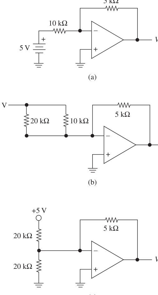
Figure P15–4
by allowing us to assume what?
Sections 15–3 and 15–4
15–6. Calculate the current through each switch and the resultant Vout in
Figure 15–4 if the number 12 is input.
D 15–7.
10k�. What values must be used for the other three resistors to ensure (b) Reconstruct the data table in Figure 15–4 with new values for Vout using the resistor values found in part (a).
15–8. What effect would doubling the 20@k� resistor have on the values 15–9. What effect would changing the reference voltage (Vref) in Figure
| 15–6(a) from | +5 | to | -5V | have on Vout? |
|---|---|---|---|---|
| 15–10. Change Vref in Figure 15–6(a) to | +2V, | and calculate Vout for |
D0 = 0,D1 = 0,D2 = 0,D3 = 1.
| 15–11. Reconstruct the data table in Figure 15–6(b) for a Vref of | +2V |
|---|---|
| instead of | +5V. |
Sections 15–5 and 15–6
15–12. Does the MC1408 DAC use a binary-weighted or an R/2R method
of conversion? 15–13. What is the purpose of the op amp in the DAC application circuit of Figure 15–7(c)? 15–14. What is the resolution of the DAC0808/MC1408 DAC shown in
Figure 15–7?
C 15–15. Calculate Vout in Figure 15–7(c) for the following input values: (b) 0011 01102 (c) 3210 (d) 3010 15–16. Sketch a partial transfer function of analog output versus digital input in Figure 15–7(c) for digital input values of 0000 0000 through 0000 0111. 15–17. How could the reference current (Iref) in Figure 15–7 be changed to 1.5 mA? What effect would that have on the range of Iout and Vout?
D 15–18. In Figure 15–7(c), if Vref is changed to 5 V, find Vout full-scale (A1 to
15–19. Draw a graph of the transfer function (digital output versus analog input) for the parallel-encoded ADC of Figure 15–11. 15–20. What is one advantage and one disadvantage of using the multiplecomparator parallel encoding method of A/D conversion? 15–21. Refer to the counter-ramp ADC of Figure 15–12. (a) What is the level at the DAC output the instant after the start conversion push button is pressed?
(b) What is the relationship between the V (+) and V (-) comparator inputs 15–22. In Figure 15–12, what is the worst-case (longest) conversion time that might be encountered if the clock frequency is 100 kHz?
Sections 15–9 and 15–10
15–23. Determine the conversion time for an 8-bit ADC that uses a
successive-approximation circuit similar to Figure 15–13 if its clock frequency is 50 kHz. 15–24. What connections could be made in the ADC shown in Figure 15–13 to enable it to make continuous conversions?
| C | 15–25. Use the SAR ADC of Figure 15–13 to convert the analog voltage | |
|---|---|---|
| of 7.28 to 8-bit binary. If | Vref = 10V, | determine the final binary answer |
and the percentage error. 15–26. Why is the three-state buffer at the output of the NE5034 ADC an important feature? 15–27. Referring to the block diagram of the ADC0804 (Figure 15–17), which inputs are used to enable the three-state output latches? Are they active-LOW or active-HIGH inputs? 15–28. What type of application might require the use of the differential
inputs [Vin(+),Vin(-)] on the ADC0804?
(a) How would the operation change if RD were connected to +5V
(b) How would the operation change if CS were connected to +5V
(c) What is the purpose of the 10@k�-0.001@mF RC circuit? 0.5 V?
C 15–30. Change VCC to 5.12 V in Figure 15–18, and determine which LEDs (a) 3.6 V (b) 1.86 V
15–31. Briefly describe the flow of the signal from the temperature transducer as it travels through the circuit to the RAM memory in the data acquisition system of Figure 15–20.
C D 15–32. Table 15–2 gives the values for the output of the thermistor circuit
| RF so that Vout equals 5 V at | 25�C. | |
|---|---|---|
| C | 15–33. The output voltage of Figure 15–22 is exactly 2.5 V at | 25�C. |
| Calculate the range of output voltage if the | 10@k� | thermistor has a toler- |
ance of 5%. 15–34. What binary value will the 8051 microcontroller read in Figure
| 15–23 if the temperature is | 60�C? | |
|---|---|---|
| C | 15–35. Through experimentation, it is determined that the strain gage in | |
| Figures 15–25 and 15–26 changes in resistance by | 20m� | for each kilo- |
gram that is added to the metal beam. Determine how many kilograms of force are on the metal beam if Vout is 4 V in Figure 15–26.
Schematic Interpretation Problems
See Appendix G for the schematic diagrams. to the 4096/4196 control card. Assume that software will be written by a programmer to output the appropriate digital strings to port 1 (P1.7–P1.0) of the 8031 microcontroller. Devise an analog output circuit using an MC1408 DAC with a 741 op amp to output analog voltages in the range of 0 to 5 V. to the 4096/4196 control card. The design must be capable of inputting the 8-bit digital results from two ADC0804 converters into port 1 (P1.7–P1.0) of the 8031 microcontroller. Assume that a single-bit control signal will be output on port 2, bit 0 (P2.0) to tell which ADC results are to be transmit-
ted. (Assume 1 = ADC1 and 0 = ADC2). Set up the ADCs for continu-
MultiSIM®Exercises
E15–1. Load the circuit file for Section 15–3a. This is a binary-weighted D/A converter like that shown in Section 15–3. (a) Close each switch individually to determine how many volts each switch contributes to Vout. List those four values in a data table. (b) The current through IF is always equal to Isum (T or F)?
MULTISIM®EXERCISES 751
(d) How many different digital numbers can be represented with the four input switches? (e) To make a 5-bit D/A you would need to add another switch and resistor to the left of D3. What size would that resistor be?
| C | E15–2. Load the circuit file for Section 15–5a. This DAC outputs a volt- | |
|---|---|---|
| age proportional to its 8-bit binary input. The | +Vref | input is set to 5 V. This |
in turn sets the maximum output at 5 V. Because there are 256 possible
binary input steps, then the volts per step will be 5V/256 = 19.53mV. The order inputs are not used in this case.) (a) On a piece of paper, sketch and label the analog output value. (b) Change the “Final” address in the Word Generator to FF so that all 256 steps will be output. Sketch and label the resultant waveform. E15–3. Load the circuit file for Section 15–10a. This ADC is used to convert the analog Vin into a binary number at the output of the ADC. This binary output is displayed in hex on the two seven-segment displays. The analog Vin is varied by changing the potentiometer setting (R and Shift-R). (a) Create a data table of analog Vin versus hex output for 11 steps in Vin from 0 to 5 V. (b) Convert all of your hex answers to decimal. Do they appear to be taking approximately equal steps?
C E15–4. Load the circuit file for Section 15–10b. The object of this design sine wave that is input to the ADC is set up to oscillate between the levels 0 and 5 V. The ADC converts the analog signal into its digital equivalent at about 30 data points. As you drag the #1 cursor the hex numbers change. (First, they increase as the sine wave increases, and then they decrease as the sine wave’s amplitude decreases.) (a) List on a piece of paper the hex digits that you read as you drag the
#1 cursor.(b) Identify the hex numbers that represent the midpoint, peak, and valley of the sine wave.
Answers to Review Questions
15–1. True 15–6. False
15–2. 256 15–7. True
15–3. Infinite, 0 15–8. Current
15–4. 240k� 15–9. A1
15–5. Because finding accurate 15–10. Number of bits at the input or
| resistances over such a large | output |
|---|---|
| range of values would be very | 15–11. True |
difficult 15–12. Gain error
15–14. 1023 15–21. False
15–15. False 15–22. True
15–16. False 15–23. True
15–17. STRT,DR 15–24. It is a linear device, whereas
15–18. False the thermistor is a nonlinear
device. 15–19. (a) Input (b) input (c) input (d) output
Comments
Leave a Reply