 ChipBuddy
← Home
ChipBuddy
← Home
Chapter 17 Microprocessor Fundamentals
OUTLINE
17–1 Introduction to System Components and Buses
17–2 Software Control of Microprocessor Systems
17–3 Internal Architecture of a Microprocessor
17–4 Instruction Execution within a Microprocessor
17–5 Hardware Requirements for Basic I/O Programming
17–6 Writing Assembly Language and Machine Language Programs
17–7 Survey of Microprocessors and Manufacturers
OBJECTIVES
Upon completion of this chapter, you should be able to do the following:
- Describe the benefits that microprocessor design has over hard-wired IC logic design.
- Discuss the functional blocks of a microprocessor-based system having basic I/O capability.
- Describe the function of the address, data, and control buses.
- Discuss the timing sequence on the three buses required to perform a simple I/O operation.
- Explain the role of software program instructions in a microprocessor-based system.
- Understand the software program used to read data from an input port and write it to an output port.
- Discuss the basic function of each of the internal blocks of the 8085A microprocessor.
- Follow the flow of data as they pass through the internal parts of the 8085A microprocessor.
- Make comparisons between assembly language, machine language, and high- level languages.
- Discuss the fundamental circuitry and timing sequence for external microprocessor I/O.
INTRODUCTION
The design applications studied in the previous chapters have all been based on combinational logic gates and sequential logic ICs. One example is a traffic light controller that goes through the sequence green–yellow–red. To implement the circuit using
shift register for sequencing the lights, and a D flip-flop if we want to interrupt the sequence with a pedestrian cross-walk push button. A complete design solution is easily within the realm of SSI and MSI ICs. Conversely, think about the complexity of electronic control of a modern automobile. There are several analog quantities to monitor, such as engine speed, manifold pressure, and coolant temperature, and there are several digital control functions to perform, such as spark plug timing, fuel mixture control, and radiator circulation control. The operation is further complicated by the calculations and decisions that have to be made on a continuing basis. This is definitely an application for a microprocessor- based system. A system designer should consider a microprocessor-based solution whenever an application involves making calculations, making decisions based on external stimulus, and maintaining memory of past events. A microprocessor offers several advantages over the hard-wired SSI/MSI IC approach. First, the microprocessor itself is a general-purpose device. It takes on a unique personality by the software program instructions given by the designer. If you want it to count, you tell it to do so, with software. If you want to shift its output level left, there’s an instruction for that. And if you want to add a new quantity to a previous one, there’s another instruction for that. Its capacity to perform arithmetic, make comparisons, and update memory makes it a very powerful digital problem solver. Making changes to an application can usually be done
by changing a few program instructions, unlike the hard-wired system that may have to be totally redesigned and reconstructed. New microprocessors are introduced every year to fill the needs of the design engineer. However, the theory behind microprocessor technology remains basically the same. It is a general-purpose digital device that is driven by software instructions and communicates with several external support chips to perform the necessary I/O of a specific task. Once you have a general understanding of one of the earlier microprocessors that came on the market, such as the Intel 8080/8085, the Motorola 6800, or the Zilog Z80, it is an easy task to teach yourself the necessary information to upgrade to the new microprocessors as they are introduced. Typically, when a new microprocessor is introduced, it will have a few new software instructions available and have some of the I/O features, previously handled by external support chips, integrated right into the microprocessor chip. Learning the basics on these new microprocessor upgrades is more difficult, however, because some of their advanced features tend to hide the actual operation of the microprocessor and may hinder your complete understanding of the system.
*17–1*Introduction to System Components and Buses
Figure 17–1 shows a microprocessor with the necessary support circuitry to perform
basic input and output functions. We use this figure to illustrate how the microprocessor acts like a general-purpose device, driven by software, to perform a specific task related to the input data switches and output data LEDs. First, let’s discuss the components of the system.
Microprocessor
The heart of the system is an 8-bit microprocessor. It could be any of the popular 8-bit microprocessors such as the Intel 8085, the Motorola 6800, or the Zilog Z80. They are called 8-bit microprocessors because external and internal data movement is performed on 8 bits at a time. It will read program instructions from memory and execute *Sections 17–1 through 17–4 are reprinted from Digital and Microprocessor Fundamentals: Theory and Applications, Fourth Edition, by William Kleitz, © 2003. Reprinted by permission of Pearson Education Inc., Upper Saddle River, NJ.
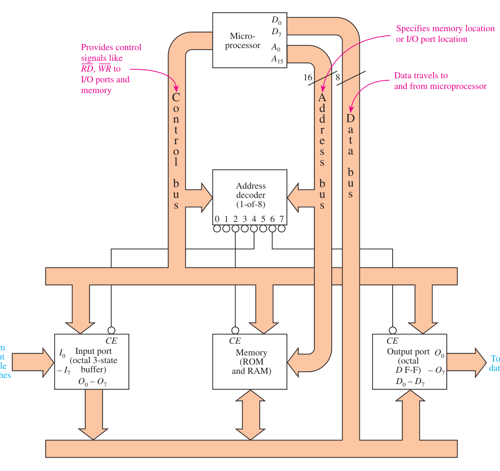
Figure 17–1 Example of a microprocessor-based system used for simple I/O operations.
those instructions that drive the three external buses with the proper levels and timing to make the connected devices perform specific operations. The buses are simply groups of conductors that are routed throughout the system and tapped into by various devices (or ICs) that need to share the information that is traveling on them.
Address Bus
The address bus is 16 bits wide and is generated by the microprocessor to select a particular location or IC to be active. In the case of a selected memory IC, the low-order bits on the address bus select a particular location within the IC (see Section 16–5). Because the address bus is 16 bits wide, it can actually specify 65,536 (216) different addresses. The input port is one address, the output port is one address, and the memory in a system of this size may be 4K (4096) addresses. This leaves about 60K addresses available for future expansion.
Data Bus
Once the address bus is set up with the particular address that the microprocessor wants to access, the microprocessor then sends or receives 8 bits of data to or from that address via the bidirectional (two-way) data bus.
Control Bus
The control bus is of varying width, depending on the microprocessor being used. It carries control signals that are tapped into by the other ICs to tell what type of operation is being performed. From these signals, the ICs can tell if the operation is a read, a write, an I/O, a memory access, or some other operation.
The address decoder is usually an octal decoder like the 74LS138 studied in Chapters 8
and 16. Its function is to provide active-LOW Chip Enables (CE) to the external ICs buses. Because there are multiple ICs on the data bus, the address decoder ensures that only one IC is active at a time to avoid a bus conflict caused by two ICs writing different data to the same bus.
Memory
There will be at least two memory ICs: a ROM or EPROM and a RAM. The ROM will contain the initialization instructions, telling the microprocessor what to do when power is first turned on. This includes tasks like reading the keyboard and driving the CRT display. It also contains several subroutines that can be called by the microprocessor to perform such tasks as time delays or I/O data translation. These instructions, which are permanently stored in ROM, are referred to as the monitor program or operating system. The RAM part of memory is volatile, meaning that it loses its contents when power is turned off and, therefore, is used only for temporary data storage.
Input Port
The input port provides data to the microprocessor via the data bus. In this case, it is an octal buffer with three-stated outputs. The input to the buffer is provided by some input device like a keyboard or, as in this case, from eight HIGH–LOW toggle switches. The input port will dump its information to the data bus when it receives a Chip Enable
(CE) from the address decoder and a Read command (RD) from the control bus. The output port provides a way for the microprocessor to talk to the outside world. It could be sending data to an output device like a printer or, as in this case, it could send data to eight LEDs. An octal D flip-flop is used as the interface because, after the microprocessor sends data to it, the flip-flop will latch on to the data, allowing the microprocessor to continue with its other tasks. To load the D flip-flop, the microprocessor must first set up the data bus with the data to be output. Then, it sets up the address of the output port so that the address de-
coder will issue a LOW CE to it. Finally, it issues a pulse on its WR (write) line that receives the clock trigger pulse, it latches onto the data that are on the data bus at that time and drives the LEDs.
Review Questions
17–1. What are the names of the three buses associated with micro-
processors? 17–2. How much of the circuitry shown in Figure 17–1 is contained inside a microcontroller IC? 17–3. Why must the data bus be bidirectional? 17–4. The purpose of the address decoder IC in Figure 17–1 is to enable two or more of the external ICs to be active at the same time to speed up processing. True or false?
its outputs are floating whenever any other IC is writing data to the data bus. True or false? 17–6. What would be the consequence of using an octal buffer for the output port in Figure 17–1 instead of an octal D flip-flop?
17–2 Software Control of Microprocessor Systems
The nice thing about microprocessor-based systems is that, once you have a working prototype, you can put away the soldering iron because all operational changes can then be made with software. The student of electronics has a big advantage when writing microprocessor software because he or she understands the hardware at work as well as the implications that software will have on the hardware. Areas such as address decoding, chip enables, instruction timing, and hardware interfacing become important when programming microprocessors. As a brief introduction to microprocessor software, let’s refer back to Figure 17–1 and learn the statements required to perform some basic I/O operations. To route the data from the input switches to the output LEDs, the data from the input port must first be read into the microprocessor before they can be sent to the output port. The microprocessor has an 8-bit internal register called the accumulator that can be used for this purpose. The software used to drive microprocessor-based systems is called assembly language. The Intel 8080/8085 assembly language statement to load the contents of the input port into the accumulator is LDA addr. LDA is called a mnemonic, an abbreviation of the operation being performed, which in this case is “Load Accumulator.” The suffix addr will be replaced with a 16-bit address (4 hex digits) specifying the address of the input port. After the execution of LDA addr, the accumulator will contain the digital value that
was on the input switches. Now, to write these data to the output port, we use the command STA addr. STA is the mnemonic for “Store Accumulator,” and addr is the 16-bit address where you want the data stored. Execution of those two statements is all that is necessary to load the value of the switches into the accumulator and then transfer these data to the output LEDs. The microprocessor takes care of the timing on the three buses, and the address decoder takes care of providing chip enables to the appropriate ICs. If the system is based on Motorola or Zilog technology, the software in this case will be almost the same. Table 17–1 makes a comparison of the three assembly languages.
TABLE 17–1 Comparison of I/O Software on Three Different Microprocessors Hint
| Operation | Intel 8080/8085 | Motorola 6800 | Zilog Z80 | |
|---|---|---|---|---|
| It is beyond the scope of | Load accumulator | this text to cover an entire | with contents of | |
| software instruction set, | location addr | LDA addr but it might be instructive | LDAA addr Store accumulator | LD A, (addr) |
| for you to locate a | to location addr | STA addr | STAA addr | LD (addr), A |
programmer’s manual for one of the more popular microprocessors to see an
17–3 Internal Architecture of a Microprocessor
entire list of instructions so that you can get a feel for
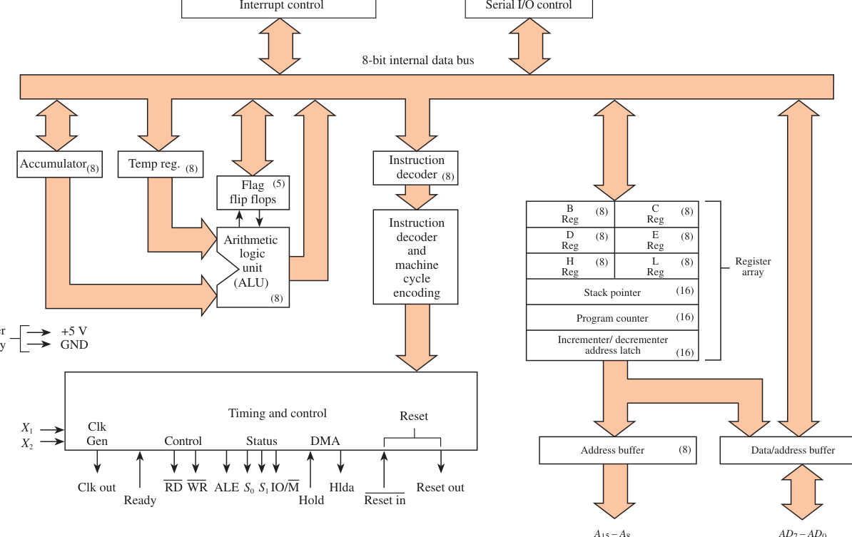
its power. The design for the Intel 8085A microprocessor was derived from its predecessor, the programs written for the 8080A can run on the 8085A without modification. The 8085A
level of hardware integration, allowing the designer to develop complete microprocessorbased systems with fewer external support ICs than were required by the 8080A. Studying the internal architecture of the 8085A in Figure 17–2 and its pin configuration in Figure 17–3 will give us a better understanding of its operation.
| Inta | Rst 6.5 | Trap | ||
|---|---|---|---|---|
| Intr | Rst 5.5 Interrupt control | Rst 7.5 Serial I/O control | SID | SOD |
| To Address bus | To Address/data bus | ||
|---|---|---|---|
| Figure 17–2 | The 8085A CPU functional block diagram. (Courtesy of Intel Corporation.) | ||
| X1 | 1 | 40 | VCC |
| X2 | 2 | 39 | HOLD |
| RESET OUT | 3 | 38 | HLDA |
| SOD | 4 | 37 | CLK (OUT) |
| SID | 5 | 36 | RESET IN |
| TRAP | 6 | 35 | READY |
| RST 7.5 | 7 | 34 | IO/M |
| RST 6.5 | 8 | 33 | S1 |
| RST 5.5 | 9 | 32 | RD |
| INTR | 10 | 31 | WR |
8085A
| INTA | 11 | 30 | ALE |
|---|---|---|---|
| AD0 | 12 | 29 | S0 |
| AD1 | 13 | 28 | A15 |
| AD2 | 14 | 27 | A14 |
| AD3 | 15 | 26 | A13 |
| AD4 | 16 | 25 | A12 |
| AD5 | 17 | 24 | A11 |
| AD6 | 18 | 23 | A10 |
| AD7 | 19 | 22 | A9 |
| VSS | 20 | 21 Figure 17–3 | A8 The 8085A pin configuration. (Courtesy of Intel Corporation.) |
tor discussed in the previous section is connected to an 8-bit internal data bus. Six other general-purpose registers labeled B, C, D, E, H, and L are also connected to the same bus. All arithmetic operations take place in the arithmetic logic unit (ALU). The accumulator, along with a temporary register, is used as input to all arithmetic operations. The output of the operations is sent to the internal data bus and to five flag flip-flops that record the status of the arithmetic operation. The instruction register and decoder receive the software instructions from external memory, interpret what is to be done, and then create the necessary timing and control signals required to execute the instruction. The block diagram also shows interrupt control, which provides a way for an external digital signal to interrupt a software program while it is executing. This is accomplished by applying the proper digital signal on one of the interrupt inputs: INTR, RSTx.x, or TRAP. Serial communication capabilities are provided via the SID and SOD I/O pins (Serial Input Data, Serial Output Data). The register array contains the six general-purpose 8-bit registers and three 16bit registers. Sixteen-bit registers are required whenever you need to store addresses. The stack pointer stores the address of the last entry on the stack. The stack is a data storage area in RAM used by certain microprocessor operations. The program counter contains the 16-bit address of the next software instruction to be executed.
The third 16-bit register is the address latch, which contains the current 16-bit address that is being sent to the address bus. The six general-purpose 8-bit registers can also be used in pairs (B–C, D–E, H–L) to store addresses or 16-bit data.
Review Questions
17–7. The suffix addr in the LDA and STA mnemonics is used to specify
the address of the accumulator. True or false? 17–8. The LDA command is used by the microprocessor to _________ (read/write) data, and the STA command is used to _________ (read/write) data. 17–9. The 8085A microprocessor has an internal accumulator and six external registers called B, C, D, E, H, and L. True or false? 17–10. The ALU block inside the 8085A determines the timing and control signals required to execute an instruction. True or false?
17–4 Instruction Execution within a Microprocessor
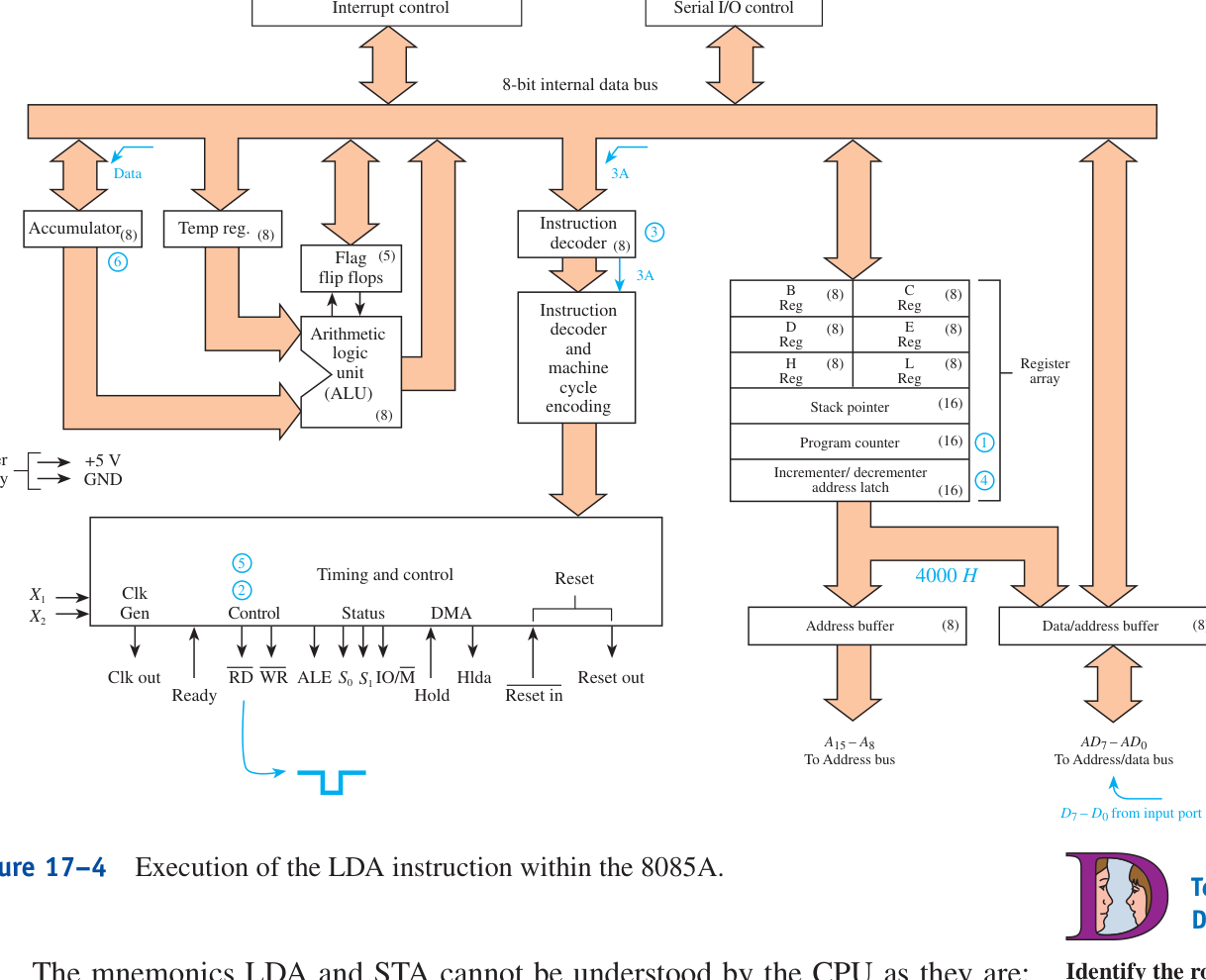
Now, referring back to the basic I/O system diagram of Figure 17–1, let’s follow the flow of the LDA and STA instructions as they execute in the block diagram of the 8085A. Figure 17–4 shows the 8085A block diagram with numbers indicating the succession of events that occurs when executing the LDA instruction. Remember, LDA addr and STA addr are assembly language instructions, stored in an external memory IC, that tell the 8085A CPU what to do. LDA addr tells the CPU to load its accumulator with the data value that is at address addr. STA addr tells the CPU to store (or send) the 8-bit value that is in the accumulator to the output port at address addr.
Interrupt control Serial I/O control
| they have to be assembled, or converted, into a binary string called machine code. | travel, from an external |
|---|---|
| Binary or hexadecimal machine code is what is actually read by the CPU and passed | input to the accumulator |
| to the instruction register and decoder to be executed. The Intel 8085A Users Manual | and then to an output port. |
gives the machine code translation for LDA as 3A16 (or 3AH) and STA as 32H.
| Before studying the flow of execution in Figure 17–4, we need to make a few as- | Common |
|---|---|
| sumptions. Let’s assume that the input port is at address 4000H and the output port is | Misconception |
| at address 6000H. Let’s also assume that the machine code program LDA 4000H, STA | Students often confuse the |
| 6000H is stored in RAM starting at address 2000H. | external data bus with the |
internal data bus.
Load Accumulator
The sequence of execution of LDA 4000H in Figure 17–4 is as follows:
- 1. The program counter puts the address 2000H on the address bus.
- 2. The timing and control unit issue a LOW pulse on the RD line. This pulse
travels the control bus to the RAM in Figure 17–1 and causes the contents at location 2000H to be put onto the external data bus. RAM (2000H) has the machine code 3AH, which travels across the internal data bus to the instruction register.
- 3. The instruction register passes the 3AH to the instruction decoder, which de-
termines that 3AH is the code for LDA and that a 16-bit (2-byte) address must follow. Because the entire instruction is 3 bytes (one for the 3AH and two for the address 4000H), the instruction decoder increments the program counter two more times so that the address latch register can read and store bytes 2 and 3 of the instruction.
| the LOW | CE | for the input port in Figure 17–1. |
|---|---|---|
| 5. The timing and control unit again issues a LOW pulse on the | RD | line. This |
pulse travels the control bus to the input port, causing the data at the input port (4000H) to be put onto the external data bus.
- 6. Those data travel across the external data bus in Figure 17–1, to the internal
data bus in Figure 17–4, to the accumulator, where they are now stored. The instruction is complete.
Store Accumulator
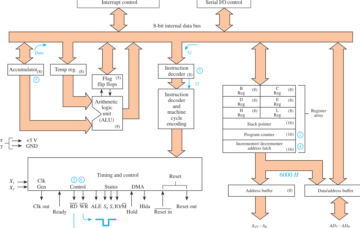
Figure 17–5 shows the flow of execution of the STA 6000H instruction.
| Inta | Rst 6.5 | Trap | ||
|---|---|---|---|---|
| Intr | Rst 5.5 Interrupt control | Rst 7.5 Serial I/O control | SID | SOD |
To Address bus To Address/data bus
Figure 17–5 Execution of the STA instruction within the 8085A.
- 1. After the execution of the 3-byte LDA 4000H instruction, the program
counter has 2003H in it. (Instruction LDA 4000H resided in locations 2000H, 2001H, 2002H.)
- 2. The timing and control unit will issue a LOW pulse on the RD line. This
causes the contents of RAM location 2003H to be put onto the external data bus. RAM (2003H) has the machine code 32H, which travels up the internal data bus to the instruction register.
- 3. The instruction register passes the 32H to the instruction decoder, which de-
termines that 32H is the code for STA and that a 2-byte address must follow. The program counter gets incremented two more times, reading and storing bytes 2 and 3 of the instruction into the address latch.
address of the output port in Figure 17–1.
- 5. The instruction decoder now issues the command to place the contents of the
accumulator onto the data bus.
- 6. The timing and control unit issues a LOW pulse on the WR line. Because the
| WR | line is used as a clock input to the D flip-flop of Figure 17–1, the data | |
|---|---|---|
| from the data bus will be stored and displayed on the LEDs. (The | WR | line |
from the microprocessor is part of the control bus in Figure 17–1.) The complete assembly language and machine code program for the preceding I/O example is given in Table 17–2.
TABLE 17–2 Assembly Language and Machine Code Listing for the
| Memory | Assembly | Machine |
|---|---|---|
| Location | Language | Code |
| 2000H | LDA 4000H | 3A |
Three-byte instruction to load accumulator
2001H 00 s
| 2002H | 40 | |
|---|---|---|
| 2003H | STA 6000H | 32 |
Three-byte instruction to store accumulator
2004H 00 s
2005H 60 17–11. What is the difference between assembly language and machine code? 17–12. Why is the instruction LDA 4000H called a 3-byte instruction? 17–13. When executing the instruction LDA 4000H, the microprocessor fetches the machine code from RAM location 4000H. True or false?
17–14. Which instruction, STA or LDA, issues a pulse on the WR line? 17–15. How many bytes of RAM does the program in Table 17–2 occupy?
17–5 Hardware Requirements for Basic I/O Programming
A good way to start out in microprocessor programming is to illustrate program execution by communicating to the outside world. In Section 17–4, we read input switches at memory location 4000H using the LDA instruction and wrote their value to output LEDs at location 6000H using the STA instruction. This was an example of memory-mapped I/O. Using this method, the input and output devices were accessed as if they were memory locations by specifying their unique 16-bit address (4000H or 6000H). The other technique used by the 8085A microprocessor for I/O mapping is called standard I/O or I/O-mapped I/O. I/O-mapped systems identify their input and
cesses the I/O ports by using the instructions OUT port and IN port, where port is 00H to FFH. Special hardware external to the 8085A is required to provide the source for the IN instruction and the destination for the OUT instruction. Figure 17–6 shows a basic hardware configuration, using standard SSI and MSI ICs, that could be built to input data from eight switches and to output data to eight LEDs using I/Omapped I/O.
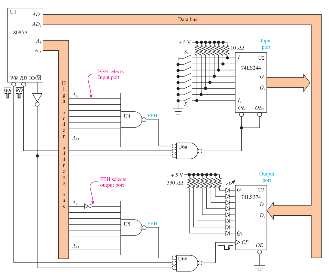
Figure 17–6 Hardware requirements for the IN FFH and OUT FEH instructions.
Figure 17–6 is set up to decode the input switches as port FFH and the output
LEDs as port FEH. The IO/M line from the microprocessor goes HIGH whenever an
memory and memory-mapped devices will cause the IO/M line to go LOW. The RD
and the WR line will be pulsed LOW when executing the OUT instruction. The 74LS244 (see Section 13–9) is an octal three-state buffer that is set up to pass the
binary value of the input switches over to the data bus as soon as OE1 and OE2 are receive three LOWs at its input. We know that the IN instruction will cause the inverted
IO/M line to go LOW and the RD line to go LOW. The other input is dependent on the binary value of the port number (1111 1111) used in the IN instruction is put onto the high-order address bus during the execution of the IN FFH instruction.
| LOW | RD | pulse), which will enable the outputs of U2 to pass to the data bus. After the |
|---|---|---|
| microprocessor drops the | RD | line LOW, it waits a short time for external devices (U2 |
| in this case) to respond, and then it reads the data bus and raises the | RD | line back |
HIGH. The data from the input switches are now stored in the accumulator.
OUT FEH
The 74LS374 (see Section 13–9) is an octal D flip-flop set up to sink current to illuminate individual LEDs based on the binary value it receives from the data bus. The outputs at Q0 to Q7 will latch onto the binary values at D0 to D7 at the LOW-to-HIGH edge of Cp. U5 and U6b are set up similarly to U4 and U6a, except U5’s output goes LOW when FEH (1111 1110) is input. Therefore, during the execution of OUT FEH,
U6b will output a LOW pulse, the same width as the WR pulse issued by the microThe setup time of the 74LS374 latch is accounted for by the microprocessor tim-
ing specifications. The microprocessor issues a HIGH-to-LOW edge at WR that makes
mulator to the data bus. After a time period greater than the setup time for U3, WR goes Q0 to Q7. To summarize, the instruction IN FFH reads the binary value at port FFH into the accumulator. The instruction OUT FEH writes the binary value in the accumulator out to port FEH. Port selection is taken care of by eight-input NAND gates attached to the
| high-order address bus and by use of the | RD,WR, | and | IO/M | lines. |
|---|---|---|---|---|
| 17–6 | Writing Assembly Language and Machine |
Language Programs
The microprocessor is driven by software instructions to perform specific tasks. The instructions are first written in assembly language using mnemonic abbreviations and then converted to machine language so that they can be interpreted by the microprocessor. The conversion from assembly language to machine language involves translating each mnemonic into the appropriate hexadecimal machine code and storing the codes in specific memory addresses. This can be done by a software package called an assembler, provided by the microprocessor manufacturer, or it can be done by the programmer by looking up the codes and memory addresses (called hand assembly). Assembly language is classified as a low-level language because the programmer has to take care of all the most minute details. High-level languages such as Pascal,
| FORTRAN, C | + | + | , and BASIC are much easier to write but are not as memory effi- |
|---|---|---|---|
| cient or as fast as assembly language. All languages, whether Pascal, C | + | + | , BASIC, or |
FORTRAN, get reduced to machine language code before they can be executed by the microprocessor. The conversion from high-level languages to machine code is done by a compiler. The compiler makes memory assignments and converts the Englishlanguage-type instructions into executable machine code. On the other hand, assembly language translates directly into machine code. This allows the programmer to write the most streamlined and memory-efficient and fastest programs possible on the specific hardware configuration that is being used. Assembly language and its corresponding machine code differ from processor to processor. The fundamentals of the different assembly languages are the same, however, and once you have become proficient on one microprocessor, it is easy to pick it up on another.
program and comparing it to the same program written in the BASIC computer lan- guage. BASIC is a high-level language that uses English-language-type commands that are fairly easy to figure out, even by the inexperienced programmer.
Program Definition
Write a program that will function as a down-counter, counting 9 to 0 repeatedly. First draw a flowchart, and then write the program statements in the BASIC language, assembly language, and machine language.
Solution
The flowchart in Figure 17–7 is used to show the sequence of program execution, including the branching and looping that takes place. Start Initialize count = 9 Decrement count
No Count Yes ?
Figure 17–7 Flowchart for Table 17–3.
According to the flowchart, the counter is decremented repeatedly until zero is reached, at which time the counter is reinitialized to 9 and the cycle repeats. The instructions used to implement the program are given in Table 17–3.
| TABLE 17–3 | Down-Counter Program in Three Languages | |||||
|---|---|---|---|---|---|---|
| 8085A | 8085A | |||||
| BASIC Language | Assembly Language | Machine Language | ||||
| Line | Instruction | Label | Instruction | Address | Contents | |
| 10 | COUNT�9 | START: | MVI A,09H | 2000 | 3E | (opcode) |
| 2001 | 09 | (data) | ||||
| 20 | COUNT�COUNT-1 | LOOP: | DCR A | 2002 | 3D | (opcode) |
| 30 | IF COUNT�0 | JZ START | 2003 | CA | (opcode) | |
| THEN GO TO 10 | 2004 | 00 | ||||
| s | (address) | |||||
| 2005 | 20 | |||||
| 40 | GO TO 20 | JMP LOOP | 2006 | C3 | (opcode) | |
| 2007 | 02 | |||||
| s | (address) | |||||
| 2008 | 20 |
BASIC uses the variable COUNT to hold the counter value. Line 30 checks the count. If COUNT is equal to zero, then the program goes back to the beginning. Otherwise, it goes back to subtract 1 from COUNT and checks COUNT again. The 8085A version of the program is first written in assembly language, and then it is either hand assembled into machine language or computer assembled using a personal computer with an assembler software package.
Assembly Language
Assembly language is written using mnemonics: MVI, DCR, JZ, and the like. The term mnemonics is defined as “abbreviations used to assist the memory.” The first mnemonic, MVI, stands for “Move Immediate.” The instruction MVI A,09H will move the data value 09H into register A (register A and the accumulator are the same). The next instruction, DCR A, decrements register A by 1. The third instruction, JZ START, is called a conditional jump. The condition that it is checking for is the zero condition. As the A register is decremented, if A reaches 0, then a flag bit, called the zero flag, gets set (a set flag is equal to 1). The instruction JZ START is interpreted as “jump to statement label START if the zero flag is set.” If the condition is not met (zero flag not set), then control passes to the next instruction, JMP LOOP, which is an unconditional jump. This instruction is interpreted as “jump to label LOOP regardless of any condition flags.” At this point you should see how the assembly language program functions exactly like the BASIC language program.
Machine Language
Machine language is the final step in creating an executable program for the microprocessor. In this step, we must determine the actual hexadecimal codes that will be stored in memory to be read by the microprocessor. First, we have to determine what memory locations will be used for our program. This depends on the memory-map assignments made in the system hardware design. We have 64K of addressable memory locations (0000H to FFFFH). We’ll make an assumption that the user program area was set up in the hardware design to start at location 2000H. The length of the program memory area depends on the size of the ROM or RAM memory IC being used. A
256 * 8 RAM memory is usually sufficient for introductory programming assignlanguage program listed in Table 17–3 fills up 9 bytes of memory (2000H to 2008H). The first step in the hand assembly is to determine the code for MVI A. This is known as the opcode (operation code) and is found in an 8085A Assembly Language Reference Chart. The opcode for MVI A is 3E. The programmer will store the binary equivalent for 3E (0011 1110) into memory location 2000H. Instructions for storing your program into memory are given by the manufacturer of the microprocessor trainer that you are using. If you are using an assembler software package, then the machine code that is generated will usually be saved on a computer disk or used to program an EPROM to be placed in a custom microprocessor hardware design. The machine language instruction MVI A,09H in Table 17–3 requires 2 bytes to complete. The first byte is the opcode, 3E, which identifies the instruction for the microprocessor. The second byte (called the operand) is the data value, 09H, which is to be moved into register A. The second instruction, DCR A, is a 1-byte instruction. It requires just its opcode, 3D, which is found in the reference chart. The opcode for the JZ instruction is CA. It must be followed by the 16-bit (2-byte) address to jump to if the condition (zero) is met. This makes it a 3-byte instruction. Byte 2 of the instruction (location 2004H) is the low-order byte of the address, and
addresses as low-order first and then high-order.) The opcode for JMP is C3 and must also be followed by a 16-bit (2-byte) address specifying the location to jump to. Therefore, this is also a 3-byte instruction where byte 2–byte 3 gives a jump address of 2002H.
17–7 Survey of Microprocessors and Manufacturers
Since its introduction in the early 1970s, the microprocessor has had a huge impact on the electronics industry. The first microprocessors had a 4-bit internal data width. In 1974, Intel introduced the first 8-bit microprocessor, the 8008. Within a year it offered an upgrade, the 8080, which served as a point of comparison for all other manufacturers. The first challenger to the 8080 was the Motorola 6800. Other IC manufacturers (National Semiconductor, Texas Instruments, Zilog, RCA, and Fairchild) soon introduced their own versions of the microprocessor. The race had begun. Since then, 16-, 32-, and 64-bit architectures have been developed and are finding their way into most new high-end applications. Along the way, manufacturers started integrating whole multichip systems with RAM, ROM, and I/O into a single package called a microcontroller. Today, the microcontroller is the most popular choice for embedded control applications such as those found in automobiles, home entertainment systems, and data acquisition and control systems. Each microprocessor and microcontroller has its own special niche, but throughout the years, the two most important players have been Intel and Motorola. Table 17–4
| TABLE 17–4 | Popular Intel and Motorola Microprocessors and Microcontrollers | ||
|---|---|---|---|
| Part | Data | Address | |
| No. | Bits | Bits | Comments |
| 8085 | 8 | 16 | Upgrade of the 8080 |
| 8051 | 8 | 16 | Microcontroller with on-chip ROM, RAM, and I/O |
| 6809 | 8 | 16 | Upgrade of the original 6800 |
| 68HC11 | 8 | 16 | Microcontroller with on-chip ROM, RAM, |
I/O, and A/D converter
| 8088 | 8 | 20 | 8-Bit downgrade of the 8086 |
|---|---|---|---|
| 8086 | 16 | 20 | Made popular by its use in IBM PC-compatible |
computers
| 80186 | 16 | 20 | 8086 with on-chip support functions |
|---|---|---|---|
| 80286 | 16 | 24 | 8086 upgrade with extended addressing capability; |
used in IBM AT-compatible computers
8096 16 16 Microcontroller with on-chip ROM, RAM,
68000 16 23 Made popular by its use in Apple Macintosh II
| 68010 | 16 | 24 | Upgrade of the 68000 |
|---|---|---|---|
| 80386 | 32 | 32 | 32-Bit upgrade of the 80286 |
| 80486 | 32 | 32 | Upgrade of the 80386 |
| 68020 | 32 | 32 | 32-Bit upgrade of the 68010 |
| 68030 | 32 | 32 | Upgrade of the 68020 |
| Pentium | 64 | 32 | Dual instruction pipelining allows concurrent |
execution of instructions, decreasing processing times
| Pentium II | 64 | 36 | Higher speeds and memory capacity |
|---|---|---|---|
| Pentium III | 64 | 36 | Upgrade of the Pentium II |
| Pentium IV | 64 | 36 | Upgrade of the Pentium III |
tify the manufacturer by the first two numbers in the part number (68 for Motorola and 80 for Intel). Appendix A lists the Web site addresses of several microprocessor manufacturers.
Review Questions
17–16. Programs written in assembly language must be converted to ma-
chine code before being executed by a microprocessor. True or false? 17–17. Programs written in a high-level language are more memory efficient than those written in assembly language. True or false? 17–18. What is the port number of the input switches and of the output LEDs in Figure 17–6? 17–19. The OUT FEH statement is used to output the switch data to the microprocessor, and the IN FFH statement is used to input data to the LEDs. True or false? 17–20. In Table 17–3, addresses 2000 through 2008 are where the _________ is stored. 17–21. How does the JZ instruction differ from the JMP instruction?
Summary of Instructions
LDA Addr: (Load Accumulator Direct) Load the accumulator with the contents of memory whose address (addr) is specified in byte 2–byte 3 of the instruction. STA Addr: (Store Accumulator Direct) Store the contents of the accumulator to memory whose address (addr) is specified in byte 2–byte 3 of the instruction. IN Port: (Input) Load the accumulator with the contents of the specified port. OUT Port: (Output) Move the contents of the accumulator to the specified port. MVI r,data: (Move Immediate) Move into register r the data specified in byte 2 of the instruction. DCR r: (Decrement Register) Decrement the value in register r by 1. JMP Addr: (Jump) Transfer control to address addr specified in byte 2–byte 3 of the instruction. JZ Addr: (Jump If Zero) Transfer control to address addr if the zero flag is set.
Summary
In this chapter, we have learned the following:
- 1. A system designer should consider using a microprocessor instead of
logic circuitry whenever an application involves making calculations, making decisions based on external stimuli, and maintaining memory of past events.
program instructions given to it by a programmer.
- 3. A microprocessor system has three buses: address, data, and control.
- 4. Microprocessors operate on instructions given to them in the form of
machine code (1s and 0s). The machine code is generated by a higher-level language like C or assembly language.
- 5. The Intel 8085A is an 8-bit microprocessor. It has seven internal regis-
ters, an 8-bit data bus, an arithmetic logic unit, and several I/O functions.
- 6. Program instructions are executed inside the microprocessor by the in-
struction decoder, which issues the machine cycle timing and initiates I/O operations.
- 7. The microprocessor provides the appropriate logic levels on the data
and address buses and takes care of the timing of all control signals output to the connected interface circuitry.
- 8. Assembly language instructions are written using mnemonic abbrevia-
tions and then converted into machine language so that they can be interpreted by the microprocessor.
- 9. Higher-level languages like C + + or Pascal are easier to write than
assembly language, but they are not as memory efficient or as fast. All languages must be converted into a machine language matching that of the microprocessor before they can be executed.
Glossary
Accumulator: The parallel register in a microprocessor that is the focal point for all arithmetic and logic operations. Address Bus: A group of conductors that are routed throughout a computer system and used to select a unique memory or I/O location based on their binary value. Architecture: The layout and design of a system. Arithmetic Logic Unit (ALU): The part of a microprocessor that performs all the arithmetic and digital logic functions. Assembler: A software package that is used to convert assembly language into machine language. Assembly Language: A low-level programming language unique to each microprocessor. It is converted, or assembled, into machine code before it can be executed. BASIC Language: A high-level computer programming language that uses Englishlanguage-type instructions that are converted to executable machine code. Bidirectional: Systems capable of transferring digital information in two directions. Central Processing Unit (CPU): The “brains” of a computer system. The term is used interchangeably with microprocessor. Compiler: A software package that converts a high-level language program into machine language code.
used to signify special control functions, such as Read, Write, I/O, Memory, and Ready. Data Bus: A group of conductors that is routed throughout a computer system and contains the binary data used for all arithmetic and I/O operations. Flowchart: A diagram used by the programmer to map out the looping and conditional branching that a program must make. It becomes the blueprint for the program. Hand Assembly: The act of converting assembly language instructions into machine language codes by hand, using a reference chart. Hardware: The ICs and electronic devices that make up a computer system. Instruction Decoder: The circuitry inside a microprocessor that interprets the machine code and produces the internal control signals required to execute the instruction. Instruction Register: A parallel register in a microprocessor that receives the machine code and produces the internal control signals required to execute the instruction. Interrupt: A digital control signal that is input to a microprocessor IC pin that suspends current software execution and performs another predefined task. I/O-Mapped I/O: A method of input/output that addresses each I/O device as a port
selected by a binary (or hex) port number. Machine Code: The binary codes that make up a microprocessor’s program instructions. Memory-Mapped I/O: A method of input/output that addresses each I/O device as a memory location selected by a binary (or hex) address. Microprocessor: An LSI or VLSI integrated circuit that is the fundamental building block of a digital computer. It is controlled by software programs that allow it to do all digital arithmetic, logic, and I/O operations. Mnemonic: The abbreviated spellings of instructions used in assembly language. Monitor Program: The computer software program initiated at power-up that supervises system operating tasks such as reading the keyboard and driving the CRT. Opcode: Operation code. It is the unique 1-byte code given to identify each instruction to the microprocessor. Operand: The parameters that follow the assembly language mnemonic to complete the specification of the instruction. Operating System: See Monitor program. Port Number: A number used to select a particular I/O port. Program Counter: An internal register that contains the address of the next program instruction to be executed. Software: Computer program statements that give step-by-step instructions to a com-
puter to solve a problem. Stack Pointer: An internal register that contains the address of the last entry on the RAM stack.
lines so that they can be referred to from different parts of the program, using statements like JUMP or CALL. Support Circuitry: The integrated circuits and electronic devices that assist the microprocessor in performing I/O and other external tasks. Zero Flag: A bit internal to the microprocessor that, when set (1), signifies the last arithmetic or logic operation had a result of zero.
Problems
Section 17–1
17–1. Describe the circumstances that would prompt you to use a microprocessor-based design solution instead of a hard-wired IC logic design. 17–2. In an 8-bit microprocessor system, how many lines are in the data bus? The address bus? 17–3. What is the function of the address bus?
D 17–4. Use a TTL data manual to find an IC that you could use for the output
| D | 17–5. Repeat Problem 17–4 for the input port. | |
|---|---|---|
| C | D | 17–6. Repeat Problem 17–4 for the address decoder. Assume that the in- |
put port is at address 4000H, the output port is at address 6000H, and memory is at address 2000H. (Hint: Use an address decoding scheme similar to that found in Section 16–5.) 17–7. Why does the input port in Figure 17–1 have to have three-stated outputs? 17–8. What two control signals are applied to the input port in Figure 17–1 to cause it to transfer the switch data to the data bus? 17–9. How many different addresses can be accessed using a 16-bit address bus?
Sections 17–2 and 17–3
17–10. In the assembly language instruction LDA 4000H, what does the
LDA signify and what does the 4000H signify? 17–11. Describe what the statement STA 6000H does. 17–12. What are the names of the six internal 8085A general-purpose registers? 17–13. What is the function of the 8085A’s instruction register and instruction decoder? 17–14. Why is the program counter register 16 bits instead of 8?
Section 17–4
| C | 17–15. During the execution of the LDA 4000 instruction in Figure 17–4, | |
|---|---|---|
| the | RD | line goes LOW four times. Describe the activity initiated by each |
LOW pulse.
instruction in Figure 17–5?
Section 17–5
17–17. Describe one advantage and one disadvantage of writing programs in a high-level language instead of assembly language. 17–18. Are the following instructions used for memory-mapped I/O or for I/O-mapped I/O?
| (a) LDA addr | (c) IN port | |
|---|---|---|
| (b) STA addr | (d) OUT port | |
| 17–19. What is the digital level on the microprocessor’s | IO/M | line for each |
of the following instructions?
| (a) LDA addr | (c) IN port |
|---|---|
| (b) STA addr | (d) OUT port |
| D | 17–20. List the new IN and OUT instructions that would be used to I/O to |
the switches and LEDs if the following changes to U4 and U5 were made in Figure 17–6. (a) Add inverters to inputs A8 and A9 of U4 and to A9 and A10 of U5. (b) Add inverters to inputs A14 and A15 of U4 and to A14 and A15 of U5. 17–21. U6a and U6b in Figure 17–6 are OR gates. Why are they drawn as inverted-input NAND gates? 17–22. Are the LEDs in Figure 17–6 active-HIGH or active-LOW?
17–23. Is the RD line or the WR line pulsed LOW by the microprocessor
(a) IN instruction? (b) OUT instruction? U2 in Figure 17–6? 17–25. What three conditions must be met to provide a pulse to the Cp input of U3 in Figure 17–6? 17–26. Which internal data register is used for the IN and OUT instructions?
Section 17–6
17–27. Write the assembly language instruction that would initialize the accumulator to 4FH. 17–28. Describe in words what the instruction JZ LOOP does.
guage program. (Start the machine code at address 2010H.)
| INIT: | MVI A,04H |
|---|---|
| X1: | DCR A |
JZ INIT JMP X1
Schematic Interpretation Problems
See Appendix G for the schematic diagrams.
S 17–30. Locate the 68HC11 microcontroller in the HC11D0 schematic. (A ports.) Pins 31–38 are the low-order address bus (A0–A7) multiplexed (shared) with the data bus (D0–D7). Pins 9–16 are the high-order address bus (A8–A15). The low-order address bus is demultiplexed (selected and latched) from the shared address/data lines by U2 and the AS (Address Strobe) line. (a) Which ICs are connected to the data bus (DB0–DB7)? (b) Which ICs are connected to the address bus (AD0–AD15)?
S C 17–31. U9 and U5 in the HC11D0 schematic are used for address decodLCD (LCD_SL) and (b) the keyboard (KEY_SL).
S 17–32. Locate the microcontroller in the 4096/4196 schematic. (b) Its low-order address is multiplexed like the 68HC11 in Problem 17–30. What IC and control signal are used to demultiplex the address/data bus (AD0–AD7) into the low-order address bus (A0–A7)? (c) What IC and control signal are used to demultiplex the address/data bus (AD0–AD7) into the data bus (D0–D7)?
MultiSIM®Exercises
E17–1. Load the circuit file for Section 17–5a. This circuit simulates the Input/Output portion of the microprocessor circuit of Figure 17–6. The object is to load the value of the input port onto the Data Bus and then send the data on the Data Bus out to the Output Port.
(a) The OE¿ on the 74LS244 must be _________ (HIGH/LOW) to load (b) Then to transfer the data on the Data Bus over to the Output Port you must _________.
(c) Change OE¿ (E) on the 74LS244 back to 1. List the order of operaOutput Port.
17–1. Address, data, control 17–12. 1 byte is used to store 3AH; 2
| 17–2. All of it | bytes are used to store 4000H. | ||
|---|---|---|---|
| 17–3. To use the same path for both | 17–13. False | ||
| input and output data | 17–14. STA, the | WR | is used as the |
| 17–4. False | clock input to the D flip-flop. | ||
| 17–5. True | 17–15. 6 bytes | ||
| 17–6. The output to the LEDs would | 17–16. True | ||
| float when | WR | returns HIGH. | 17–17. False |
| 17–7. False | 17–18. Input is FFH, output is FEH. | ||
| 17–8. Read, write | 17–19. False | ||
| 17–9. False | 17–20. Machine code | ||
| 17–10. False | 17–21. The JZ instruction looks for a | ||
| 17–11. Assembly language, which is | zero flag and jumps to the | ||
| written in short mnemonics, | label START if the flag is set. | ||
| needs to be assembled or con- | The JMP instruction jumps to | ||
| verted into a binary string | the label LOOP, regardless of | ||
| called a machine code, which | any flags. |
is read by the CPU.
Comments
Leave a Reply