 ChipBuddy
← Home
ChipBuddy
← Home
Chapter 18 The 8051 Microcontroller
OUTLINE
18–1 The 8051 Family of Microcontrollers
18–2 8051 Architecture
18–3 Interfacing to External Memory
18–4 The 8051 Instruction Set
18–5 8051 Applications
18–6 Data Acquisition and Control System Application
18–7 Conclusion
OBJECTIVES
Upon completion of this chapter you should be able to do the following:
- Describe the advantages that a microcontroller has over a microprocessor for control applications.
- Describe the functional blocks within the 8051 microcontroller.
- Make comparisons between the different microcontrollers available within the 8051 family.
- Write the software instructions to read and write data to and from the I/O ports.
- Describe the use of the alternate functions on the I/O ports.
- Make the distinction between the internal and external data and code memory spaces.
- Use various addressing modes to access internal data memory and the Special Function Registers (SFRs).
- Interface an external EPROM and a RAM to the 8051.
- Use some of the more commonly used instructions of the 8051 instruction set.
- Write simple 8051 I/Os programs.
- Use the bit operations of the 8051.
- Understand program solutions to applications such as a keyboard decoder and analog-to-digital converter. *Chapter 18 is reprinted from Digital and Microprocessor Fundamentals: Theory and Applications, Fourth Edition; by William Kleitz, © 2003. Reprinted by permission of Pearson Education Inc., Upper Saddle River, NJ. †Visit the following sites for microcontroller trainers and downloadable software tools: www.acebus.com, www.bipom.com, www.elexp.com, www.emacinc.com, and www.8052.com
In the previous chapter you should have recognized several common components that are incorporated into most microprocessor-based system applications. These are the microprocessor, RAM, ROM (or EPROM), and parallel I/O ports. Microprocessor manufacturers have recognized this and over the years since the introduction of the 8085A have been developing a new line of microprocessors specifically designed for control applications. They are called microcontrollers. The microcontroller has the CPU, RAM, ROM, timer/counter, and parallel and serial I/O ports fabricated into a single IC. It is often called “a computer on a chip.” The CPU’s instruction set is improved for control applications and offers bit-oriented data manipulation, branching, and I/O, as well as multiply and divide instructions. The microcontroller is most efficiently used in systems that have a fixed program for a dedicated application. A microcontroller is used in a keyboard for a personal computer to scan and decode the keys. It is used in an automobile for sensing and controlling engine operation. Other dedicated applications such as microwave ovens, videocassette recorders, gas pumps, and automated teller machines use the microcontroller IC also. The previous chapters have provided a good background for understanding the microcontroller. The theory behind microprocessor buses, external memory, and I/O ports is necessary to utilize the features available on a microcontroller. In this chapter we’ll be introduced to one of the most widely used microcontrollers available: the
- 8051. You’ll see several similarities between it and the 8085A-based systems previ-
ously discussed. You should appreciate the way that you were eased into microprocessor operational theory using the 8085A, but now you will see why the 8051 can be a much better solution to dedicated control applications. Most control applications require extensive I/O and need to work with individual bits. The 8051 addresses both of these needs by having 32 I/O lines and a CPU instruction set that handles single-bit I/O, bit manipulation, and bit checking.
18–1 The 8051 Family of Microcontrollers
The basic architectural structure of the 8051 is given in Figure 18–1. The block diagram gives us a good picture of the hardware included in the 8051 IC. For internal
memory it has a 4K * 8 ROM and a 128 * 8 RAM. It has two 16-bit counter/timers RXD (transmit and receive), and it also has four 8-bit parallel I/O ports (P0, P1, P2, P3). There is also an 8052 series of microcontrollers available that has an 8K ROM, 256 RAM, and three counter/timers. Other versions of the 8051 are the 8751, which has an internal EPROM for program storage in place of the ROM, and the 8031, which has no internal ROM, but instead accesses an external ROM or EPROM for program instructions. Table 18–1 summarizes the 8051 family of microcontrollers. Note that the 8052/8752/8032 series has an extra 4K of program space (except the 8032), double the RAM area, an extra timer/counter, and one additional interrupt source. All parts use the same CPU instruction set. The ROMless versions (8031 and 8032) are the least expensive parts but require an external ROM or EPROM such as a 2732 or 2764 for program storage.
18–2 8051 Architecture
To squeeze so many functions on a single chip, the designers had to develop an architecture that uses the same internal address spaces and external pins for more than one function. This technique is similar to that used by the 8085A for the multiplexed
AD0-AD7 lines.
Figure 18–1 Block diagram of the 8051 microcontroller.
TABLE 18–1 The 8051 Family of Microcontrollers
| Device | Timers/event | Interrupt | ||||||||
|---|---|---|---|---|---|---|---|---|---|---|
| number | Program | Data | counters | sources | ||||||
| 8051 | 4K | * | 8 ROM | 128 | * | 8 RAM | 2 | * | 16-bit | 5 |
| 8751H | 4K | * | 8 EPROM | 128 | * | 8 RAM | 2 | * | 16-bit | 5 |
| 8031 | None | 128 | * | 8 RAM | 2 | * | 16-bit | 5 | ||
| 8052AH | 8K | * | 8 ROM | 256 | * | 8 RAM | 3 | * | 16-bit | 6 |
| 8752BH | 8K | * | 8 EPROM | 256 | * | 8 RAM | 3 | * | 16-bit | 6 |
| 8032AH | None | 256 | * | 8 RAM | 3 | * | 16-bit | 6 |
The 8051 is a 40-pin IC. Thirty-two pins are needed for the four I/O ports. To provide for the other microcontroller control signals, most of those pins have alternate functions, which are described in this section. Also in this section, we see how the 8051 handles the overlapping address spaces used by internal memory, external memory, and the special function registers. The pin configuration for the 8051 is given in Figure 18–2.
Port 0
Port 0 is dual-purpose, serving as either an 8-bit bidirectional I/O port (P0.0–P0.7) or
the low-order multiplexed address/data bus (AD0-AD7). As an I/O port, it can sink up
(IOL = 3.2mA). The alternate port designations, AD0-AD7, are used to access exter-
memory. The AD lines are demultiplexed into A0-A7 and D0-D7 by using the ALE
Port 1
Port 1 is an 8-bit bidirectional I/O port that can sink or source up to 4 LS TTL loads.
(IOL = 1.6mA and IOH = -80mA.)
Figure 18–2 The 8051 pin configuration.
Port 2
Port 2 is dual-purpose, serving as either an 8-bit bidirectional I/O port (P2.0–P2.7) or
as the high-order address bus (A8-A15) for access to external memory. As an I/O port address bus whenever reference to external memory is made.
Port 3
Port 3 is dual-purpose, serving as an 8-bit bidirectional I/O port that can sink or source up to 4 LS TTL loads or as special-purpose I/O to provide the functions listed in Table 18–2.
| TABLE 18–2 | Alternative Functions of Port 3 | |
|---|---|---|
| Port pin | Alternative function | |
| P3.0 | RXD (serial input port) | |
| P3.1 | TXD (serial output port) | |
| P3.2 | INT0 | (external interrupt 0) |
| P3.3 | INT1 | (external interrupt 1) |
| P3.4 | T0 (Timer 0 external input) | |
| P3.5 | T1 (Timer 1 external input) | |
| P3.6 | WR | (external data memory write strobe) |
| P3.7 | RD | (external data memory read strobe) |
RST
Reset input. A HIGH on this pin resets the microcontroller.
ALE/ PROG
Address Latch Enable output pulse for latching the low-order byte of the address dur-
ing accesses to external memory. This pin is also the program pulse input (PROG) dur-
Program Store Enable is a read strobe for external program memory. It will be con-
| nected to the Output Enable | (OE) | of an external ROM or EPROM. |
|---|---|---|
| EA | /VPP | |
| External Access | (EA) | is tied LOW to enable the microcontroller to fetch its program |
code from an external memory IC. This pin also receives the 21-V programming supply voltage (VPP) for programming the EPROM parts.
XTAL1,XTAL2
Connections for a crystal or an external oscillator.
Address Spaces
The address spaces of the 8051 are divided into four distinct areas: internal data memory, external data memory, internal code memory, and external code memory (see
Figure 18–3).
The 8051 allows for up to 64K of external data memory (RAM) and 64K of external code memory (ROM/EPROM). The only disadvantage of external memory, in addition to the additional circuitry, is that ports 0 and 2 get tied up for the address and data bus. The actual hardware interfacing for external memory are given later in this chapter. When the 8051 is first reset, the program counter starts at 0000H. This points to
| the first program instruction in the internal code memory unless | EA | (External Access) | ||
|---|---|---|---|---|
| is tied LOW. If | EA Figure 18–3 | is tied LOW, the CPU issues a LOW on 8051 address spaces. | PSEN | (Program Store |
LOW if using the ROMless (8031) version.
With EA tied HIGH, the first 4K of program instruction fetches are made from FFFFH) will automatically be made from the external code memory. If the application has a need for large amounts of data memory, then external data memory (RAM) can be used. I/O to external RAM can only be made by using one of the MOVX instructions. When executing a MOVX instruction, the 8051 knows that
you are referring to external RAM and issues the appropriate WR or RD signal. memory is better to use because it has a much faster response time and a broad spectrum of instructions to access it. Figure 18–3 shows two blocks of internal data memory. The first is the 128-byte RAM at address 00H to 7FH. The second is made up of the Special Function Registers (SFRs) at addresses 80H to FFH. Note that all addresses are only 1 byte wide, which allows for more efficient use of code space and faster access time. The use of the address space in the 128-byte RAM is detailed in
Figure 18–4.
The first 32 locations are set aside for four banks of data registers (called register banks), giving the programmer the use of 32 separate registers. The registers within each bank are labeled R0 through R7. The bank that is presently in use is defined by the setting of the two “bank select bits” in the PSW (Program Status Word).
Figure 18–4 Address space in the 128-byte internal data memory RAM.
locations. This meets the needs of control applications for a large number of ON/OFF bit flags, by providing 128 uniquely addressable bit locations. The last 80 locations are set aside for general-purpose data storage and stack operations. The Special Function Registers are maintained in the next 128 addresses in the internal data memory of the 8051 (address 80H to FFH). It contains registers that are required for software instruction execution as well as those used to service the special hardware features built into the 8051. Table 18–3 lists the SFRs and their addresses. The address of an SFR is also only 1 byte wide. However, instead of specifying the 1-byte hex address, you also have the option of addressing any SFR location by simply specifying its register name, like P0 or SP. Several of the SFRs are bit addressable. For example, to address bit 3 of the accumulator, you would use the address E0H.3 (or you could use ACC.3). The PSW is also bit addressable, having the bit addresses listed in Table 18–4. For example, to address the parity bit in the PSW, you would use the address D0H.0 (or you could use PSW.0).
TABLE 18–3 The Special Function Registers (SFRs) [Internal Data
| Register | Address | Function |
|---|---|---|
| P0 | 80Ha | Port 0 |
| SP | 81H | Stack pointer |
| DPL | 82H | Data pointer (Low) |
| DPH | 83H | Data pointer (High) |
| TCON | 88Ha | Timer register |
| TMOD | 89H | Timer mode register |
| TL0 | 8AH | Timer 0 low byte |
| TL1 | 8BH | Timer 1 low byte |
| TH0 | 8CH | Timer 0 high byte |
| TH1 | 8DH | Timer 1 high byte |
| P1 | 90Ha | Port 1 |
| SCON | 98Ha | Serial port control register |
| SBUF | 99H | Serial port data buffer |
| P2 | A0Ha | Port 2 |
| IE | A8Ha | Interrupt enable register |
| P3 | B0Ha | Port 3 |
| IP | B8Ha | Interrupt priority register |
| PSW | D0Ha | Program status word |
| ACC | E0Ha | Accumulator (direct address) |
| B | F0Ha | B register |
aBit-addressable register.
| TABLE 18–4 | The PSW Bit Addresses | |
|---|---|---|
| Symbol | Address | Function |
| CY | D0H.7 | Carry flag |
| AC | D0H.6 | Auxiliary carry flag |
| F0 | D0H.5 | General-purpose flag |
| RS1 | D0H.4 | Register bank select (MSB) |
| RS0 | D0H.3 | Register bank select (LSB) |
| OV | D0H.2 | Overflow flag |
| — | D0H.1 | User-definable flag |
| P | D0H.0 | Parity flag |
Up to 64K of code memory (ROM/EPROM) and 64K of data memory (RAM) can be added to any of the 8051 family members. If you are using the 8031 (ROMless) part, then you have to use external code memory for storing your program instructions. As mentioned earlier, the alternate function of port 2 is to provide the high-order address
| byte | (A8-A15), | and the alternate function of port 0 is to provide the multiplexed low- |
|---|---|---|
| order address/data byte | (AD0-AD7). |
If you are interfacing to a general-purpose EPROM like the 2732, then the ALE
signal provided by the 8031 is used to demultiplex the AD0-AD7 lines via an address As you can see, two of the I/O ports are used up to provide the address and data
buses. The AD0-AD7 lines that are output on port 0 are demultiplexed by the ALE sig-
lier. The PSEN signal is asserted at the end of each instruction fetch cycle to enable the
The EA line is tied LOW so that the 8031 knows to fetch all program code from exter-
Figure 18–5 Interfacing a 2732 EPROM to the ROMless 8031 microcontroller.
can be used. The 8155 RAM accepts the lines directly and uses the ALE to use 11 of the 8051 pins to interface to the 8155, but the 8155 provides an additional 22 I/O lines, giving us a net gain of 11. The addresses of the external RAM locations are 0000H to 00FFH, overlapping the addresses of the internal data memory. There is not a conflict, however, because all I/O to the external data memory is made using the MOVX instruction. The MOVX instruction ignores internal memory and, instead, activates the appropriate control sig-
nal, RD or WR via port 3. The LOW RD or WR signal allows the 8155 to send or
The I/O ports on the 8155 are accessed by making the IO/M line HIGH. This is (8000H or higher).
Figure 18–6 Interfacing an 8155 RAM/IO/Timer to the 8051 microcontroller.
All the members of the 8051 family use the same instruction set. (The complete instruction set is given in the 8051 Instruction Set Summary in Appendix H.) Several new instructions in the 8051 make it especially well suited for control applications. The discussion that follows assumes that you are using a commercial assembler software package. Hand assembly of the 8051 instructions into executable machine code is very difficult and misses out on several of the very useful features available to the ASM51 programmer.
Addressing Modes
The instruction set provides several different means to address data memory locations. We’ll use the MOV instruction to illustrate several common addressing modes. For example, to move data into the accumulator, any of the following instructions could be used:
MOV A,Rn: Register addressing, the contents of register Rn (where n = 0-7) MOV A,@Ri: Indirect addressing, the contents of memory whose address is in
Ri (where i = 0 or 1) is moved to the accumulator. (Note: Only registers R0 and MOV A,20H: Direct addressing, move the contents of RAM location 20H to the accumulator. I/O ports can also be accessed as a direct address as shown in the following instruction. MOV A,P3: Direct addressing, move the contents of port 3 to the accumulator. Direct addressing allows you to specify the address by giving its actual hex address (e.g., B0H) or by giving its abbreviated name (e.g., P3), which is listed in the SFR table (Table 18–3). MOV A,#64H: Immediate constant, move the number 64H into the accumulator. In each of the previous instructions, the destination of the move was the accumulator. The destination in any of those instructions could also have been a register, a direct address location, or an indirect address location.
EXAMPLE 18–1
Write the 8051 instruction to perform each of the following operations. (a) Move the contents of the accumulator to register 5. (b) Move the contents of RAM memory location 42H to port 1. (c) Move the value at port 2 to register 3. (d) Send FFH to port 0. (e) Send the contents of RAM memory, whose address is in register 1, to port 3.
Solution:
(a) MOV R5,A (b) MOV P1,42H (c) MOV R3,P2
is because the ASM51 assembler requires that the first position of any hexadecimal number must be a numeric digit from 0 to 9.) (e) MOV P3,@R1
Program Branching Instructions
8051 assembly language provides several different ways to branch (jump) to various program segments within the 64K of code memory area. Below are some of the most useful jump instructions. JMP label (Unconditional jump): Program control passes to location label. The JMP instruction is converted by the ASM51 assembler into an absolute jump, (AJMP), a short jump (SJMP), or a long jump (LJMP), depending on the destination pointed to by label. JZ label (Jump if accumulator zero): Program control passes to location label if the accumulator equals zero. JNZ label (Jump if accumulator not zero): Program control passes to location label if the accumulator is not equal to zero. JB bit,label (Jump if bit set): Program control passes to location label if the specified bit, bit, is set. JNB bit,label (Jump if bit not set): Program control passes to location label if the specified bit, bit, is not set. DJNZ Rn,label (Decrement register and jump if not zero): Program control passes to location label if, after decrementing register Rn, the register is not
equal to zero (n = 0-7). equal): Program control passes to location label if register Rn is not equal to the immediate data #data. The compare can also be made to the accumulator by specifying A instead of Rn. CALL label (Call subroutine): Program control passes to location label. The return address is stored on the stack. The CALL instruction is converted by the ASM51 assembler into an absolute call, ACALL, or a long call, LCALL, depending on the destination pointed to by label. RET (Return): Program control is returned back to the instruction following the CALL instruction.
EXAMPLE 18–2
Write a program that continuously reads a byte from port 1 and writes it to port 0 until the byte read equals zero.
Solution:
| READ: | MOV A,P1 | ; A | d | P1 |
|---|---|---|---|---|
| MOV P0,A | ; P0 JNZ READ | d ; Repeat until A | A = NOP | 0 ; Remainder of program |
etc.
Repeat Example 18–2, except stop the looping when the number 77H is read.
Solution:
| READ: | MOV A,P1 | ; A | d | P1 |
|---|---|---|---|---|
| MOV P0,A | ; P0 | d CJNE A,#77H,READ | A ; Repeat until NOP | A = 77H ; Remainder of program |
etc.
EXAMPLE 18–4
Repeat Example 18–2, except stop the looping when bit 3 of port 2 is set.
Solution:
| READ: | MOV A,P1 | ; A | d | P1 |
|---|---|---|---|---|
| MOV P0,A | ; P0 | d | A JNB P2.3,READ NOP etc. | ; Repeat until bit 3 of port 2 is set ; Remainder of program ; |
EXAMPLE 18–5
Write a program that will produce an output at port 0 that counts down from 80H to 00H.
Solution:
| MOV R0,#80H | ; R0 | d | 80H | |
|---|---|---|---|---|
| COUNT: | MOV P0,R0 | ; P0 DJNZ R0,COUNT NOP etc. | d ; Decrement R0, jump to COUNT if not 0 ; Remainder of program ; | R0 |
Logical and Bit Operations
The 8051 instruction set provides the basic logical operations (OR, AND, Ex-OR, and NOT), rotates (left or right, with or without carry), and bit operations (Clear, Set, and complement). The following list shows some of the most commonly used of those operations. ANL A,Rn (AND register to accumulator): Logically AND register Rn, bit by bit, with the accumulator and store the result in the accumulator. ANL A,#data (AND data byte to accumulator): Logically AND data byte #data, bit by bit, with the accumulator and store the result in the accumulator.
use the following instructions: ORL A,Rn (OR register to accumulator) ORL A,#data (OR data byte to accumulator) XRL A,Rn (Ex-OR register to accumulator) XRL A,#data (Ex-OR data byte to accumulator) The most commonly used instructions to operate on individual bits are as follows: CLR bit (Clear bit): Clear (reset to 0) the value of the bit located at address bit. SETB bit (Set bit): Set (set to 1) the value of the bit located at address bit. CPL bit (Complement bit): Complement the value of the bit located at address bit. The rotate commands available to the 8051 programmer are as follows: RL A (Rotate accumulator left): Rotate the 8 bits of the accumulator one position to the left. RLC A (Rotate accumulator left through carry): Rotate the 9 bits of the accumulator including carry one position to the left. RR A (Rotate accumulator right): Rotate the 8 bits of the accumulator one position to the right. RRC A (Rotate accumulator right through carry): Rotate the 9 bits of the accumulator including carry one position to the right. The following examples illustrate the use of the logical and bit operations.
EXAMPLE 18–6
Determine the contents of the accumulator after the execution of the following program segments.
| (a) MOV A,#3CH | ; A | d | 0011 1100 |
|---|---|---|---|
| MOV R4,#66H | ; R4 | d | 0110 0110 |
| ANL A,R4 | ; A | d | A AND R4 |
Solution:
A = 00111100 R4 = 01100110
AANDR4 = 00100100 = 24H Answer
| (b) MOV A,#3FH | ; A | d | 0011 1111 |
|---|---|---|---|
| XRL A,#7CH | ; A | d | EX-OR 7CH |
Solution:
A = 0011 1111 7CH = 0111 1100
A EX@OR 7CH = 0100 0011 = 43H Answer
RR A ; Rotate right A = 1010 0011 Rotate right
A = 1101 0001 Answer
| (d) MOV A,#0C3H | ; A | d | 1100 0011 |
|---|---|---|---|
| RLC A | ; Rotate left through carry |
Solution:
Assume carry = 0 initially A = 1100 0011 Rotate left through carry
A = 1000 0110, carry = 1 Answer
EXAMPLE 18–7
Use the SETB, CLR, and CPL instructions to do the following operations: (a) Clear bit 7 of the accumulator. (b) Output a 1 on bit 0 of port 3. (c) Complement the parity flag (bit 0 of the PSW).
Solution:
(a) CLR ACC.7 (Note: According to Table 18–3, the symbol for the direct address of the accumulator is ACC.) (b) SETB P3.0 (c) CPL PSW.0
EXAMPLE 18–8
Describe the activity at the output of port 0 during the execution of the following program segment: MOV R7,#0AH MOV P0,#00H
LOOP: CPL P0.7 Solution: Register 7 is used as a loop counter with the initial value of 10 (0AH). Each time that the complement instruction (CPL) is executed, bit 7 will toggle to its opposite state. Toggling bit 7 ten times will create a waveform with five positive pulses.
The 8051 is capable of all the basic arithmetic functions: addition, subtraction, incrementing, decrementing, multiplication, and division. The following list outlines the most commonly used forms of the arithmetic instructions. ADD A,Rn (Add register to accumulator): Add the contents of register Rn
(where n = 0-7) to the accumulator and place the result in the accumulator. the accumulator and place the result in the accumulator. SUBB A,Rn (Subtract register from accumulator with borrow): Subtract the contents of register Rn and borrow (carry flag) from the accumulator and place the result in the accumulator. SUBB A,#data (Subtract immediate data from accumulator with borrow): Subtract the value of #data and borrow (carry flag) from the accumulator and place the result in the accumulator. INC A (Increment accumulator) INC Rn (Increment register) DEC A (Decrement accumulator) DEC Rn (Decrement register) MUL AB (Multiply A times B): Multiply the value in the accumulator times the value in the B register. The low-order byte of the 16-bit product is left in the accumulator and the high-order byte is placed in register B. DIV AB (Divide A by B): Divide the value in the accumulator by the value in the B register. The accumulator receives the quotient and register B receives the remainder. DA A (Decimal adjust accumulator): Adjust the value in the accumulator, resulting from an addition, into two BCD digits.
The following examples illustrate the use of arithmetic instructions.
EXAMPLE 18–9
Add the value being input at port 1 to the value at port 2 and send the result to port 3.
Solution:
| MOV R0,P1 | ; R0 | d | P1 | ||
|---|---|---|---|---|---|
| MOV A,P2 | ; A | d | P2 | ||
| ADD A,R0 | ; A | d | A | + | R0 |
| MOV P3,A | ; P3 | d | A |
EXAMPLE 18–10
Multiply the value being input at port 0 times the value at port 1 and send the result to ports 3 and 2 (high order/low order).
| MOV A,P0 | ; A | d | P0 |
|---|---|---|---|
| MOV B,P1 | ; B | d | P1 |
| MUL AB | ; A | * | B |
| MOV P2,A | ; P2 | d | A (low order) |
| MOV P3,B | ; P3 | d 18–5 | B (high order) 8051 Applications |
Having bit-handling instructions and built-in I/O makes the 8051 a good choice for data acquisition and control applications. In this section we look at a few applications that illustrate how we can utilize these new features to simplify our program solutions.
Instruction Timing
The 8051 circuitry that we looked at earlier was driven with a 12-MHz crystal. The 12 MHz is a convenient choice because each instruction machine cycle takes 12 clock periods
to complete. This means that one machine cycle takes 1ms. All 8051 instructions are DIV, which take four. The oscillator periods for each instruction are given in the 8051 Instruction Set Summary (Appendix H). For example, the MOV A,Rn instruction
requires 12 oscillator periods to complete, which will take 1ms [12 * (1/12MHz)]. Knowing the time duration of each instruction, we can write accurate time delays for our applications programs. Writing counter/loop programs is much easier now, with the introduction of the DJNZ and the CJNE instructions. Table 18–5 and Figure 18–7 show a time-delay program that we could call as a subroutine from an applications program.
| TABLE 18–5 | Time-Delay Subroutine | |||
|---|---|---|---|---|
| DELAY: | MOV R1,#0F3H | ; Outer-loop counter (F3H | = | 243) |
| MOV R0,#00H | ; Inner-loop counter | |||
| LOOP: | DJNZ R0,LOOP | ; Loop 256 times | ||
| DJNZ R1,LOOP | ; Loop 243 times | |||
| RET | ; Return | |||
| The DJNZ instruction takes 24 oscillator periods, or 2 s. By initializing regis- | m |
ter 0 at 00H, the first time DJNZ R0,LOOP is executed, R0 will become FFH. The program will loop within that same instruction 255 more times until R0 equals 0. At that point, control drops down to the next DJNZ, which functions as an outer loop as shown in the flowchart.
The R0 (inner) loop will take 512 s to complete. The R1 (outer) loop exe- m second. A third loop, using R2, could be added to increase the time by another factor of 256.
Figure 18–7 Flowchart for the time-delay subroutine of Table 18–5.
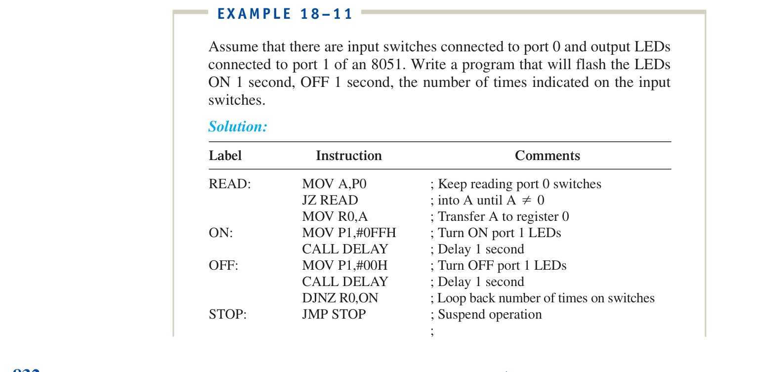
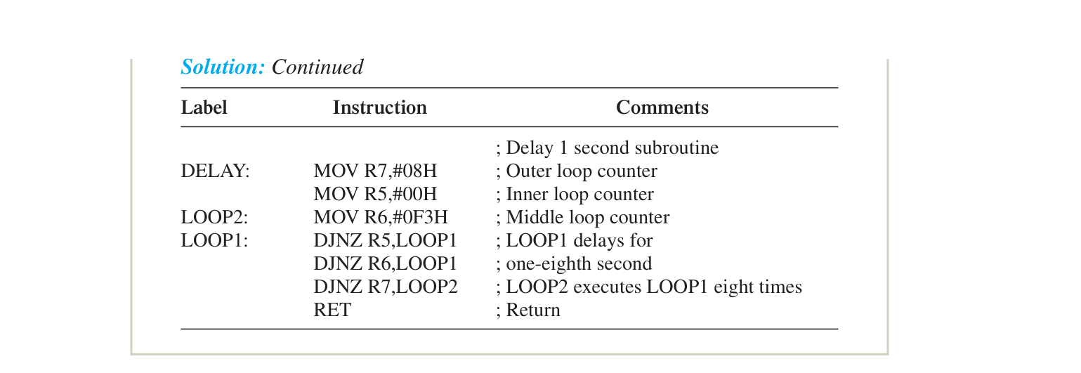
EXAMPLE 18–12
Write a program that will decode the hexadecimal keyboard shown in
Figure 18–8.
Solution:
| Label | Instruction | Comments |
|---|---|---|
| KEYSCAN: | CALL ROWRD CALL COLRD CALL CONVRT | ; Determine row of key pressed ; Determine column of key pressed ; Convert row/column to key value |
| STOP: | JMP STOP | ; Suspend operation |
;
| ROWRD: | MOV P0,#0FH | ; Output 0s to all columns | |
|---|---|---|---|
| MOV R0,#00H | ; Row JNB P0.0,RET1 | = ; Return if row 0 is LOW | 0 |
| MOV R0,#01H | ; Row JNB P0.1,RET1 | = ; Return if row 1 is LOW | 1 |
| MOV R0,#02H | ; Row JNB P0.2,RET1 | = ; Return if row 2 is LOW | 2 |
| MOV R0,#03H | ; Row JNB P0.3,RET1 JMP ROWRD | = ; Return if row 3 is LOW ; Else keep reading | 3 |
| RET1: | RET | ; Return |
;
| COLRD: | MOV P0,#0F0H | ; Output 0s to all rows | |
|---|---|---|---|
| MOV R1,#00H | ; Column JNB P0.4,RET2 | = ; Return if column 0 is LOW | 0 |
| MOV R1,#01H | ; Column JNB P0.5,RET2 | = ; Return if column 1 is LOW | 1 |
| MOV R1,#02H | ; Column JNB P0.6,RET2 | = ; Return if column 2 is LOW | 2 |
| MOV R1,#03H | ; Column JNB P0.7,RET2 JMP COLRD | = ; Return if column 3 is LOW ; Else keep reading | 3 |
| RET2: | RET | ; Return |
;
| CONVRT: | MOV B,#04H | ; B | = | Multiplication factor | |||
|---|---|---|---|---|---|---|---|
| MOV A,R0 | ; Move row number to A | ||||||
| MUL AB | ; A | = | row | * | 4 | ||
| ADD A,R1 | ; A | = | row RET | * ; A now contains value of key pressed | 4 | + | column |
Figure 18–8 Keyboard interface to an 8051.
Explanation: The keyboard is wired as a 4 * 4 row–column matrix. order is connected to the columns. The rows and columns are held HIGH
with the 10@k� pull-up resistors. Because the I/O ports of the 8051 can nique to scan a keyboard than we would use with the 8085A. To determine the row of a depressed key, we drive all of the columns LOW and all of the rows HIGH by executing the instruction MOV P0,#0FH. The HIGH on the rows is actually a float state, allowing the rows to be read. The next series of instructions in the ROWRD subroutine read each row to determine the row number that is LOW, if any. If, for example, key 5 is depressed, then row 1 will be LOW and the other three rows will be HIGH. Now that we know the row, we must next determine the column. The instruction MOV P0,#0F0H will drive the rows LOW and float the columns. If the number 5 key is still depressed, column 1 will be LOW. The last subroutine converts the row–column combination to the numeric value of the key pressed. Rows 0, 1, 2, and 3 have weighting factors of 0, 4, 8, and 12, respectively, and columns 0, 1, 2, and 3 have weighting factors of 0, 1, 2, and 3, respectively. Knowing that, the CONVRT subroutine uses the following formula to determine the numeric value of the key pressed: Keypressed = row * 4 + column
EXAMPLE 18–13
Figure 18–9 shows how an ADC0801 (or ADC0804) is interfaced to an
- 8051. Write a program that takes care of the handshaking requirements for
SC and EOC to complete an analog-to-digital conversion.
Figure 18–9 Interfacing an analog-to-digital converter to an 8051.
Solution:
| Label | Instruction | Comments | ||
|---|---|---|---|---|
| FLOAT: | MOV P1,#0FFH MOV P0,#0FFH | ; Write 1s to port 1 ; Write 1s to port 0 | ||
| SC: | CLR P0.6 SETB P0.6 | ; Output LOW-then-HIGH on ; | SC | |
| WAIT: | JB P0.7, WAIT | ; Wait here until | EOC | goes LOW |
| DONE: | MOV R0,P1 | ; Transfer ADC result to register 0 |
Explanation: The I/O ports are in the float condition after the initial reset of the 8051. They must be floating to be used as inputs. The first two instructions in this program write 1s to ports 1 and 0, which make them float just in case they had 0s in them from a previous step in the program.
To start the conversion process, bit 6 of port 0 (SC) is pulsed LOW then
if-bit-set instruction (JB) then monitors bit 7 of port 0 (EOC) and remains 1 is read into register 0, which is used to hold the ADC result.
18–6 Data Acquisition and Control System Application
The object of this section is to implement the 8051-based data acquisition and control system shown in Figure 18–10. Three modules are discussed using several external transducers and instruments as follows:
Figure 18–10 Modular 8051-based data acquisition and control application.
- 1. ADC module with hex display of the output.
- 2. DAC module with hex display of the input.
- 3. 8051 microcontroller module with connection points for (1) and (2).
Assembly-language software will be written and stored on an EPROM connected to the 8051. This software will exercise the ADC/DAC modules and perform other I/O functions. One of the outcomes of these designs is for their use in colleges for teaching the concepts of data acquisition and control, so careful attention will be paid to the cost, durability, and ease of reproduction of each module.
Hardware
The 8051 Microcontroller Module The 8051 microcontroller module is shown in ule are input and output buffers, an address latch, and an EPROM interface. In Figure 18–11, the microcontroller used is the 8031, which is a subset of the
- 8051. The 8031 differs in that it is the ROM-less part. Instead of using the 8051, which
has an internal mask-programmable ROM, we use the 8031 and interface an EPROM to it to supply our program statements. The 8031 will be run with a 12-MHz crystal. This was chosen because most of the instructions take 12 clock periods to execute. This way, accurate timing can be
developed based on 1@ms instruction execution time. required to access the EPROM comes from the 8 bits provided from port 0 and the 4 bits provided from port 2. The data output from the EPROM are sent back into the microcontroller via port 0. Because port 0 has a dual purpose (i.e., address and data), a control signal from the ALE line is used to tell the address latch when port 0 has valid
addresses and when it has data. Also, the EA signal is grounded, which signifies that the microcontroller is ready to read data from the EPROM. This LOW control signal is
attached to the OE line of the 2732 EPROM, which changes the outputs at D0 through reads the data.
Hardware reset is provided at pin 9 via the R-C circuit of R1 – C3. At power-up the HIGH-to-LOW level for PIN 9 to be reset. Resetting can also be accomplished with the push-button, which shorts the 5-V supply directly to pin 9 any time you want to have a user reset. Two eight-bit I/Os are provided via port 1 and port 3. In this circuit, port 1 is used as an output port capable of sinking or sourcing up to four LSTTL loads. This is equivalent to a sink current of approximately 1.6 mA, which is normally not enough to drive loads such as LED indicators. Because of this, the 74LS244 (U1) is used as an output buffer. The 74LS244 can sink 24 mA and source 15 mA. The outputs of this buffer are always enabled by grounding pins 1 and 19. This way, whatever appears at port 1 will immediately be available to the LEDs. The LEDs are connected as active-LOW by pro-
viding a series 270 ohm resistor to the 5-V supply. When any of the outputs of U1 go +
8051 Microcontroller with input/output.
on this module so that other devices can be driven from this port at the same time that the LEDs are being activated. In this circuit, port 3 is used for input. The 8-bit DIP switch is connected to port 3 in conjunction with the 10K DIP pack. Therefore, each of the bits of port 3 is normally HIGH via a 10K pull-up. They are made LOW any time one of the DIP switches is closed. An input socket is also provided at this port so that external digital inputs can be input to port 3. To use the input socket, all eight of the DIP switches must be in their open position so that the devices driving the input socket can drive the appropriate line LOW or HIGH without a conflict with the LOW from the DIP switch. The 74LS373 is an octal transparent latch used as an address demultiplexer. Data entered at the D inputs are transferred into the Q outputs whenever the LE input is HIGH. The data at the D inputs are latched when the LE goes LOW. This address latch is used to demultiplex port 0s address/data information. When port 0 has valid address information, the ALE line is pulsed HIGH. This causes the address latch to grab hold of the information on port 0 and pass it through to the Qs and latch onto it. After the addresses from port 0 are latched, the port is then placed in the float condition so that it can be used to receive the data from the EPROM as the PSEN line is pulsed LOW.
The LOW pulse on the PSEN line activates the active-LOW OE on the EPROM, which microcontroller, where they are used as program instructions.
The ADC Interface Module The heart of the ADC interface module (Figure 18–12) and can be directly interfaced to a microcontroller. The object of this interface module
is to convert analog quantities brought into Vin(+) into 8-bit digital outputs. The digital microcontroller module. They are also connected to the 2-digit hex display so that you can constantly monitor the 8-bit values that were converted.
| The clock oscillator for the ADC is provided via | R19C1. | The frequency of oscil- |
|---|---|---|
| lation can be calculated by taking the reciprocal of | (1.1 * 10k�* 150pF), | which |
equals approximately 606 kHz. Because this is a successive approximation ADC we can assume that the conversion will take place in 10 to 12 clock periods, which provides a conversion time of about 20 ms. The chip select (CS) pin on U1 is connected to ground so that the chip is always activated. The RD pin is an active-LOW output enable. This is connected to ground
| also, so that the outputs are always active. To start a conversion, the | WR | line, which is |
|---|---|---|
| also known as the start-conversion | (SC), | is pulsed LOW-then-HIGH. After the SAR |
has completed its conversion, it issues a LOW pulse on the INTR line [also known as
end-of-conversion (EOC) ], which will be read by the microcontroller to determine if
| The | Vref/2 | pin is connected to a reference voltage that overrides the normal refer- |
|---|---|---|
| ence of 5 V provided by Vcc. By setting the | Vref/2 | at 1.28 volts, the actual Vref will be |
2.56 V. This way, with a Vref of 2.56 V, and an ADC that has a maximum number of steps of 256, the change in the output will be 1 bit change or 1 binary step for every 10 mV of input change. This provides a convenient conversion for the linear temperature sensor (T1) because T1 provides a 10 mV change for every degree Celsius. It also makes the calculations for the linear phototransistor sensor much simpler.
The DAC Interface Module The heart of the DAC interface module (Figure 18–13)
verted are brought into the A8-A1 digital input side with A1 receiving the MSB. The
| The amount of full-scale output current is dictated by the | R1-R2 | reference resistors. |
|---|---|---|
| With a 15 V supply and a | 10@k� | resistor, the maximum output current will be 1.5 mA. |
The ADC 0804 interface module.
The MC1408 DAC interface module.
this current-to-voltage conversion, a 741 op amp is used. The current at Io is drawn
| through the | 10@k� | feedback resistor of U2. This way, the analog Vout is equal to Io |
|---|---|---|
| times | 10k�. | The analog output voltage can be predicted by using a ratio method. The |
ratio of the analog Vout to the binary input is proportional to the ratio of the maximum analog Vout to the maximum binary input (15 V maximum divided by 256 maximum).
(Because the supply on the op amp is ; 15V, we will never be able to achieve 15 V A two-digit hexadecimal display is connected directly to the input to the DAC chip. This provides a way to monitor the binary input at any time.
Applications
Three separate applications are used to exercise the three modules. Each of these applications are controlled by the microcontroller and will read analog input values with the ADC and output analog values with the DAC.
Celsius Thermometer The Celsius thermometer application is shown in Figure to the ADC and display a binary coded decimal (BCD) output of the temperature. The LM35 linear temperature sensor is used to measure the temperature. It outputs 10 mV for every degree Celsius. This millivolt value is converted by the ADC into an 8-bit binary string, which is displayed on the hex display and also input to the microcontroller. Because the Vref on the ADC is set at 2.56 V, the output of the ADC is an actual hexadecimal display of the degrees Celsius. The microcontroller is used to start the ADC conversion and then monitor the
end of conversion (EOC) line to wait for the conversion to be complete. Once the conthe hexadecimal value into a BCD value so that it can be read by the user on the display of the DAC module. The analog output value of the DAC is not used. The ASM51 software used by this application is given in Table 18–6. This listing basically has five columns. The first lists the memory locations 0000–0062 that are programmed in the EPROM. The next shows the actual hex contents of the memory locations, starting with 802E and continuing down through 22. The third and fourth show the assembly language programming with labels starting with the ORG 0008H and ending with the RET statement. In the extreme right-hand column is the comments section for the program. As you read through the comments section you will see that three subroutines are used to call the three different operations that are going to take place. The first subroutine, ADC, is used to float the buses on port 3 and port 1 and then issue the start con-
version (SC) signal. The “wait” part of that subroutine is necessary to wait until EOC After the ADC routine is complete and the digital value is stored in register 0, that value in register 0 must be converted from hex to BCD. To do this, a counter
Figure 18–14 Celsius thermometer.
| Addr | Hex | Label | ASM51 | Comments |
|---|---|---|---|---|
| 0000 | ORG | 0000H | ; START OF EPROM | |
| 0000 | 802E | SJMP | START | ; SKIP OVER 8051 RESTART |
; LINK AREA
| 0030 | ORG | 0030H | ; START OF PGM | ||
|---|---|---|---|---|---|
| 0030 | 1138 | START: | ACALL | ADC | ; PERFORM AN A-TO-D |
; CONVERSION
0032 1159 ACALL DAC ; DISPLAY RESULT AND ; CONVERSION
| 0034 | 114C | ACALL | DELAY | ; DELAY 4 SECOND |
|---|---|---|---|---|
| 0036 | 80F8 | SJMP | START | ; REPEAT |
;
| 0038 | 75B0FF | ADC: | MOV | P3,#0FFH | ; FLOAT THE BUS | ||
|---|---|---|---|---|---|---|---|
| 003B | 7590FF | MOV | P1,#0FFH | ; FLOAT THE BUS | |||
| 003E | C2B7 0040 | SC: D2B7 | CLR SETB | P3.7 P3.7 | ; DROP ; THEN RAISE HIGH | SC | LINE LOW |
| 0042 | 20B6FD 0045 0047 0049 | WAIT: C2B6 C2B7 A8B0 | JB CLR CLR MOV | P3.6, WAIT P3.6 ; USED FOR P3.7 ; USED FOR R0,P3 | ; WAIT TILL ; CLEAR P3.6 WHICH WAS EOC ; CLEAR P3.7 WHICH WAS SC ; STORE FINAL ADC RESULT | EOC | GOES LOW |
; INTO R0
004B 22 RET
| 004C | 7F20 | DELAY: | MOV | R7,#20H | ; OUTERMOST LOOP (32 times) |
|---|---|---|---|---|---|
| 004E | 7D00 | MOV | R5,#00H | ; INNERMOST LOOP (256 times) | |
| 0050 | 7EF3 | LOOP2: | MOV | R6,#0F3H | ; MIDDLE LOOP (243 times) |
| 0052 | DDFE 0054 0056 | LOOP1: DEFC DFF8 | DJNZ DJNZ DJNZ 0058 | R5,LOOP1 R6,LOOP1 R7,LOOP2 22 | ; ; ; RET |
; CONVERT HEX TO BCD ; AND DISPLAY ON DAC ; MODULE
| 0059 | 7400 | DAC: | MOV | A,#00H | ; ZERO OUT ACCUMULATOR |
|---|---|---|---|---|---|
| 005B | 2401 | LOOP3: | ADD | A,#01H | ; Acc WILL HAVE VALID BCD, |
; R0=ADC HEX ; RESULT
005D D4 DA A ; DECIMAL ADJUST Acc IF
005E D8FB DJNZ R0,LOOP3 ; DECR R0 WHILE INCR AND ; R0=0
0060 F590 MOV P1,A ; MOV CORRECTED BCD TO
0062 22 RET ;
0000 END
accumulator will have in it the correct BCD value that was achieved by using the decimal adjust instruction (DA A). After the DAC displays the BCD result, a delay is used for approximately 4 seconds so that there will be a 4-second delay before the temperature is refreshed.
Temperature-Dependent PWM Speed Control This application is shown in Figure this application is to monitor the temperature and produce a pulse-width-modulated (PWM) square wave whose duty cycle is proportional to the temperature. This PWM square wave can be used to drive a DC motor. The effective DC value will increase as the duty cycle increases. Because the duty cycle increases with increasing temperature, the speed of the motor will also increase with increasing temperature. The ASM51 software used to drive this application is given in Table 18–7. Basically, this software has two subroutines that are called. The first one is the ADC subroutine. This subroutine starts the conversion, waits until the conversion is complete, and moves the ADC result into register 0. The next subroutine, the PWM, is used to produce the PWM square wave. To produce a PWM square wave, the output of the DAC will first be held LOW (0 V) for a delay multiple equivalent to 10 hexadecimal. Then the DAC will be sent HIGH, which in this case is one-half the full-scale output (80 hex). This HIGH is held for a delay multiple equivalent to the temperature value received from the ADC conversion. This way, as the ADC result increases with increasing temperature, the duty cycle of the PWM will increase, thus increasing the effective DC value sent to the motor.
Integrating Solar Radiometer The block diagram for the integrating solar radiometensity and produce a real-time display of the irradiation from the sunlight and then accumulate the irradiation, the same as taking the integral, and display the integrated output as an analog voltage and also on a hex display. To measure the irradiation, an ECG 3034 phototransistor is used. It produces 300 nA per microwatt per centimeter
squared. The current is changed to a voltage by the 330- � resistor. This analog voltgram. The integrated output of the ADC will be proportional to the amount of sunlight that struck the measured surface over a certain length of time. This length of time could be one hour, one day, one week, or whatever time is desired. The software used to execute this application is given in Table 18–8. The first subroutine is the ADC subroutine, which is used to convert the irradiation into a digital value. After the microcontroller has this digital value, the DAC routine performs the integration simply by accumulating the ADC result over each period of time. The DAC provides both the hexadecimal equivalent of the integrated irradiation as well as an analog output voltage that is proportional to the integrated irradiation.
Figure 18–15 Temperature-dependent PWM speed control.
| Addr | Hex | Label | ASM51 | Comments |
|---|---|---|---|---|
| 0000 | ORG | 0000H | ; START OF EPROM | |
| 0000 | 8030 | SJMP | START | ; SKIP OVER 8051 RESTART |
; LINK AREA
| 0030 | ORG | 0030H | ; START OF PGM | ||
|---|---|---|---|---|---|
| 0030 | 7F01 | START: | MOV | R7,#01H | ; TO ENABLE ADC READ ON |
; 1st LOOP
0032 1138 LOOP: ACALL ADC ; PERFORM AN A-TO-D
0034 114C ACALL PWM ; DRIVE DC MOTOR WITH
| 0036 | 80FA | SJMP | LOOP | ; REPEAT | |
|---|---|---|---|---|---|
| 0038 | DF11 | ADC: | DJNZ | R7,ERET | ; TAKE AN ADC READ EVERY |
; 256th TIME FOR ; STABILITY
| 003A | 75B0FF | MOV | P3,#0FFH | ; FLOAT THE BUS | |||
|---|---|---|---|---|---|---|---|
| 003D | C2B7 | SC: | CLR | P3.7 | ; DROP | SC | LINE LOW |
| 003F | D2B7 | SETB | P3.7 | ; THEN RAISE HIGH |
; (PROVIDES POSITIVE EDGE)
| 0041 | 20B6FD | WAIT: | JB | P3.6,WAIT | ; WAIT TILL | EOC | GOES LOW |
|---|---|---|---|---|---|---|---|
| 0044 | E5B0 | MOV | A,P3 | ; STORE ADC RESULT INTO |
; Acc
| 0046 | 547F | ANL | A,#01111111B | ; CLEAR BIT 7 WHICH WAS |
|---|---|---|---|---|
| ; USED FOR | SC | |||
| 0048 | F8 | MOV | R0,A | ; MOVE ADC RESULT TO |
; REG 0
0049 AF40 MOV R7,40H ; RESET REG 7 to 64 DECIMAL
004B 22 ERET: RET
| 004C | 759000 | PWM: | MOV | P1,#00H | ; OUTPUT A LOW |
|---|---|---|---|---|---|
| 004F | 743F | MOV | A,#3FH | ; 3FH IS HIGHEST ASSUMED |
; ADC OUTPUT VALUE
0051 98 SUBB A,R0 ; SUBTRACT THE ADC
0052 F9 MOV R1,A ; R1 (DELAY VALUE) FOR
| 0053 | 115D | ACALL | DELAY | ; CALL DELAY TO HOLD LOW |
|---|---|---|---|---|
| 0055 | 7590FF | MOV | P1,#0FFH | ; OUTPUT FULL SCALE |
; OUTPUT FOR A HIGH
0058 A900 MOV R1,R0 ; USE TEMPERATURE AS ; FOR HIGH
005A 115D ACALL DELAY ; CALL DELAY TO HOLD
005C 22 RET ; RETURN
| 005D | 7D80 | DELAY: | MOV | R5,#80H | ; START COUNT OF R5 |
|---|---|---|---|---|---|
| 005F | DDFE | LOOP1: | DJNZ | R5,LOOP1 | ; R5=INNERLOOP COUNT |
; DOWN TO ZERO
0061 D9FA DJNZ R1,DELAY ; R1=MULTIPLIER FROM
| 0063 | 22 | RET |
|---|---|---|
| 0000 | END |
Figure 18–16 Integrating solar radiometer.
| TABLE 18–8 | Integrating Solar Radiometer Software | |||
|---|---|---|---|---|
| Addr | Hex | Label | ASM51 | Comments |
| 0000 | ORG | 0000H | ; START OF EPROM | |
| 0000 | 8030 | SJMP | START | ; SKIP OVER 8051 RESTART |
; LINK AREA
| 0030 | ORG | 0030H | ; START OF PGM | ||
|---|---|---|---|---|---|
| 0030 | 7400 | START: | MOV | A,#00H | ; RESET ACCUMULATOR |
| 0032 | 113A | LOOP: | ACALL | ADC | ; PERFORM AN A-TO-D |
; CONVERSION
0034 1158 ACALL DAC ; DISPLAY RESULT AND ; CONVERSION
| 0036 | 114B | ACALL | DELAY | ; DELAY 4 SECOND | |||
|---|---|---|---|---|---|---|---|
| 0038 | 80F8 | SJMP | LOOP | ; REPEAT | |||
| 003A | 75B0FF | ADC: | MOV | P3,#0FFH | ; FLOAT THE BUS | ||
| 003D | C2B7 | SC: | CLR | P3.7 | ; DROP | SC | LINE LOW |
| 003F | D2B7 | SETB | P3.7 | ; THEN RAISE HIGH | |||
| 0041 | 20B6FD | WAIT: | JB | P3.6,WAIT | ; WAIT TILL | EOC | GOES LOW |
| 0044 | C2B6 | CLR | P3.6 ; USED FOR | ; CLEAR P3.6 WHICH WAS EOC | |||
| 0046 | C2B7 | CLR | P3.7 ; USED FOR | ; CLEAR P3.7 WHICH WAS SC | |||
| 0048 | A8B0 | MOV | R0,P3 | ; STORE FINAL ADC RESULT |
; INTO R0
004A 22 RET
| 004B | 7F20 | DELAY: | MOV | R7,#20H | ; OUTERMOST LOOP (32X) |
|---|---|---|---|---|---|
| 004D | 7D00 | MOV | R5,#00H | ; INNERMOST LOOP (256X) | |
| 004F | 7EF3 | LOOP2: | MOV | R6,#0F3H | ; MIDDLE LOOP (243X) |
| 0051 | DDFE 0053 0055 | LOOP1: DEFC DFF8 | DJNZ DJNZ DJNZ 0057 | R5,LOOP1 R6,LOOP1 R7,LOOP2 22 | ; ; ; RET |
; INTEGRATE BY ACCUMU; LATING ADC RESULT
0058 8840 DAC: MOV 40H,R0 ; MOVE ADC RESULT TO
005A 53403F ANL 40H,#00111111B ; MASK OFF UNWANTED
005D 2540 ADD A,40H ; ACCUMULATE NEW ADC ; TOTAL
| 005F | F590 | MOV | P1,A | ; MOVE TO DAC DISPLAY |
|---|---|---|---|---|
| 0061 | 22 | RET | ; |
;
0000 END
This three-module method for data acquisition and control proves to be a very inexpensive and simple way to be able to input both analog and digital quantities and to output both digital and analog quantities. Having the hex displays connected to the input and output modules is an effective way of monitoring the real-time activity of the DAC and the ADC. The entire three-module data-acquisition setup is very portable in that it requires only a bipolar power supply to operate it. The software used to exercise these modules is very straightforward and is effectively written using the ASM51 assembler on a personal computer and downloaded to an EPROM using a standard EPROM programming software package. Once you have the programmed EPROM, all that is required for a stand-alone data acquisition system is a power supply.
Summary
In this chapter we have learned the following:
- 1. The 8051 microcontroller is different from a microprocessor because it
has the CPU, ROM, RAM, timer/counter, and parallel and serial ports fabricated into a single IC.
- 2. Thirty-two of the 40 pins of the 8051 are used for the four 8-bit parallel
I/O ports. Three of the ports share their function with the address, data, and control buses.
- 3. The address spaces of the 8051 are divided into four distinct areas: in-
ternal data memory, external data memory, internal code memory, and external code memory. The internal data memory is further divided into user RAM and Special Function Registers (SFRs).
- 4. To interface to an external EPROM like the 2732, an octal D-latch is
required to demultiplex the address/data bus, which is shared with port 0.
The External Access (EA) pin is tied LOW and the (PSEN) output is used
- 5. Extra data memory and I/O ports can be interfaced by using the 8155
IC. The 8155 demultiplexes the address/data bus internally so an octal D-latch is not required.
- 6. The MOV instruction is very powerful, providing the ability to move
data almost anywhere internal or external to the microcontroller and to the I/O ports.
7. Program branching is accomplished by use of many different condi-
tional and unconditional jumps and calls.
- 8. The 8051 instruction set provides the ability to work with individual
bits, which makes it very efficient for on/off control operations. Instructions are available for all the logic functions, rotates, and bit manipulations.
- 9. Instructions are provided for all the basic arithmetic instructions: addi-
tion, subtraction, multiplication, division, incrementing, and decrementing.
- 10. Each instruction machine cycle takes 12 clock periods to complete.
This means that if a 12-MHz crystal is used, each machine cycle takes 1 s m
single I/O port.
- 12. Interfacing an 8-bit analog-to-digital converter to an 8051 is accom-
plished with one port and two bits on a second port. The start-conversion LOW pulse is issued with bit-setting instructions and the end-of-conversion signal is monitored with bit-checking instructions.
Glossary
Assembler: A software package used to convert assembly language programs into executable machine code. Bidirectional: An I/O port that can be used for both input and output. Bit Addressable: Memory spaces in the internal RAM and SFR areas that allow for the addressing of individual bits.
External Access (EA): An active-LOW input that when forced LOW, tells the procesMicrocontroller: A computer on a chip. It contains a CPU, ROM, RAM, counter/ timers, and I/O ports. It is especially well suited for control applications.
Program Store Enable (PSEN): An active-Low output control signal issued by the Register Bank: A group of eight registers. The 8051 has four sets of banks that are selected by writing to the two bank-select bits in the PSW. Special Function Register (SFR): A data register that has a dedicated space within the microcontroller. It is used to maintain the data required for microcontroller operations.
Problems
18–1. Why is a microcontroller sometimes referred to as a “computer on a chip”? 18–2. Describe the difference between the 8031, 8051, and the 8751. 18–3. What additional features does the 8052 have over the 8051? 18–4. Port 2 has a dual purpose. One is as a bidirectional I/O port. What is its other purpose? 18–5. If you are using the internal ROM in the 8051 for your program code
memory, should the EA be tied HIGH or LOW? to the 8051? 18–7. What is the address range of the Special Function Registers (SFRs)? 18–8. What are the SFR addresses of the four I/O ports? 18–9. The 8051 has four register banks with eight registers in each bank. How does the CPU know which bank is currently in use?
ing the 2732 EPROM in Figure 18–5 but not when interfacing the 8155 RAM in Figure 18–6? 18–11. Determine the value of the accumulator after the execution of instruction A:, B:, C:, and D: MOV 40H,#88H MOV R0,#40H
| B: | MOV A,@R0 | ; A = _____ |
|---|---|---|
| C: | MOV A,40H | ; A = _____ |
| D: | MOV A,#40H | ; A = _____ |
18–12. Repeat Problem 18–11 for the following instructions:
MOV 50H,#33H MOV 40H,#22H MOV R0,#30H MOV 30H,50H MOV R1,#40H
| B: | MOV A,@R0 | ; A = _____ |
|---|---|---|
| C: | MOV A,R1 | ; A = _____ |
| D: | MOV A,30H | ; A = _____ |
18–13. Write the instructions to perform each of the following operations: (a) Output a C7H to port 3. (b) Load port 1 into register 7. (c) Load the accumulator with the number 55H. (d) Send the contents of RAM memory, whose address is in register 0, to the accumulator. (e) Output the contents of register 1 to port 0. 18–14. Write a program that continuously reads port 0 until the byte read equals A7H. At that time, turn on the output LEDs connected at port 1. 18–15. Write a program that will produce an output at port 1 that counts up from 20H to 90H repeatedly. 18–16. Determine the value of the accumulator after the execution of instruction A:, B:, and C: MOV A,#00H MOV R0,#36H
| B: | ORL A,#71H | ; A = _____ |
|---|---|---|
| C: | ANL A,#0F6H | ; A = _____ |
18–17. Repeat Problem 18–16 for the following program:
MOV A,#77H
| B: | SETB ACC.7 | ; A = _____ |
|---|---|---|
| C: | RL A | ; A = _____ |
18–18. Modify one instruction in Example 18–8 so that it will output eight pulses at port 0 instead of five.
outputs the result to port 1. 18–20. What is the length of time of the following time-delay subroutine? (Assume a 12-MHz crystal is being used.)
DELAY: MOV R1,#00H
LOOP: DJNZ R0,LOOP RET
Schematic Interpretation Problems
See Appendix G for the schematic diagrams. 18–21. Find Port 2 (P2.7–P2.0) of U8 in the 4096/4196 schematic. This
port outputs the high-order address bits for the system (A8-A15). On a sep-
A8-A11 to the four bits A12-A15. The HIGH output for an equal compari18–22. Locate the microcontroller in the 4096/4196 schematic. (a) What is its grid location and part number? (b) Its low-order address is multiplexed. What IC and control signal is
| used to demultiplex the address/data bus | (AD0-AD7) | into the low- |
|---|---|---|
| order address bus | (A0-A7) | ? |
Appendix A Web Sites
Useful Web sites for this book include the following: www.acebus.com (AceBus) Downloadable 8051 microcontroller editor, assembler, and simulator www.ahinc.com/scsi.htm (Advanced Horizons, Inc.) SCSI, CD, and DVD definitions and standards www.allegromicro.com (Allegro MicroSystems, Inc.) Hall Effect Sensors and Power ICs www.altera.com (Altera Corporation) CPLDs and FPGAs www.ocf.berkeley.edu/~amanb/8085.html 8085 simulator www.amd.com (Advanced Micro Devices, Inc.) Microprocessors, EPROMs, and Flash memory www.analog.com (Analog Devices, Inc.) Analog ICs, ADCs, and DACs www.bipom.com (BiPom Electronics, Inc.) Downloadable 8051 microcontroller editor, assembler, and simulator www-03.ibm.com/chips/ (IBM Microelectronics Corporation) Microprocessors, SRAMs, DRAMs, and custom logic www.datasheetcatalog.com pdf datasheet downloads www.digikey.com Sales catalog of electronic products and components www.educypedia.be/electronics Free circuit schematics, information and tutorials www.elexp.com (Electronics Express, Inc.) Sales of electronic products, CPLD
programmer boards, and microprocessor trainers and components www.emacinc.com (EMAC, Inc.) Microprocessor and microcontroller trainers and single-board computers www.fairchildsemi.com (Fairchild Semiconductor, Inc.) Digital Logic ICs, analog ICs, discrete semiconductors, EEPROMs, and microcontrollers www.fujitsumicro.com (Fujitsu, Inc.) Microcontrollers, DRAMs, and Flash memory
memories, EEPROMs, digital logic ICs, analog ICs, and discrete semiconductors www.howstuffworks.com (HowStuffWorks) Beginners guide to the operation of electronic and computer hardware and software www.idt.com (Integrated Device Technology, Inc.) SRAMs and digital logic ICs www.intel.com (Intel Corporation) Microprocessors, microcontrollers, and Flash memory www.interactiv.com (Interactive Image Technology, Inc.) Multisim®software www.intersil.com (Intersil Corporation) Analog ICs, ADCs, DACs, SRAMs, microprocessors, microcontrollers, and discrete semiconductors www.jameco.com Sales catalog of electronic products and components www.jdr.com Sales catalog of electronic products and components www.latticesemi.com (Lattice Semiconductor Corporation) CPLDs www.linear-tech.com (Linear Technology Corporation) ADCs and DACs www.microchip.com (Microchip Technology, Inc.) EEPROMs and microcontrollers www.micronsemi.com (Micron Semiconductor Products, Inc.) DRAMs, SRAMs, and Flash memory www.mot-sps.com (Motorola Semiconductors, Inc.) Analog ICs, digital logic ICs, microcontrollers, microprocessors, SRAMs, and discrete semiconductors www.mp3-tech.org (MP3 Tech) MP3 definitions and standards www.national.com (National Semiconductor Corp.) Analog ICs, digital logic ICs, and microcontrollers
www.ni.com (National Instruments, Inc.) Provider of Multisim simulation software and LabView measurement and control software www.nxp.com (NXP Semiconductors N.V.) Digital and Mixed Signal logic ICs www.onsemi.com (ON Semiconductor, Inc.) Analog ICs, digital logic ICs, and discrete semiconductors www.pctechguide.com (PCTechGuide) Technicians guide to PC hardware and software www.semiconductors.philips.com (Philips Semiconductors, Inc.) Analog ICs, digital logic ICs, microcontrollers, and discrete semiconductors www.sharpmeg.com (Sharp Microelectronics Corporation) Microprocessors, microcontrollers, SRAMs, and Flash memory www.terasic.com Provider of Altera FPGA Development and Education boards like the DE-x series www.ti.com (Texas Instruments, Inc.) Analog ICs, digital logic ICs, and microcontrollers www.toshiba.com (Toshiba America, Inc.) Analog ICs, digital logic ICs, microcontrollers, DRAMs, SRAMs, and Flash memory www.usb.org (Universal Serial Bus) USB definitions and standards www.webopedia.com Glossary of PC and internet terms with links to other sites www.xess.com (XESS Corporation) CPLD programmer boards www.xilinx.com (Xilinx, Inc.) CPLDs and FPGAs www.zilog.com (Zilog Inc.) Microprocessors and microcontrollers
Appendix B Manufacturers’ Data Sheets*
| Data Sheet IC Numbers | Function |
|---|---|
| 74HC00 | High-speed CMOS NAND |
| 74LV00 | Low-voltage NAND |
| 74ABT244 | BiCMOS Octal Buffer |
| KA741 | Operational Amplifier |
| LM555 | Timer |
| EP2C FPGA | Altera Cyclone II family |
Web Site Links to Complete Data Sheets and Useful
Reference Material
NXP Semiconductors [Formerly Philips (Signetics) Semiconductor]
74F00 NAND http://www.nxp.com/documents/data_sheet/
74F112 Flip-Flop http://www.nxp.com/documents/data_sheet/
74HC/HCT00 NAND http://ics.nxp.com/products/hc/datasheet/
74LV00 Low-V NAND http://www.nxp.com/documents/data_sheet/
74ABT244 Buffer http://www.nxp.com/documents/data_sheet/ *Courtesy of NXP Semiconductors, Fairchild Semiconductors, Xilinx, Inc., and Altera Corporation.
| LM555 | Timer | http://www.fairchildsemi.com/ds/LM/LM555.pdf |
|---|---|---|
| KA741 | Op-Amp | http://www.fairchildsemi.com/ds/KA/KA741.pdf |
National Semiconductor
| ADC0801 | ADC | http://cache.national.com/ds/AD/ADC0801.pdf |
|---|---|---|
| DAC0800 | DAC | http://cache.national.com/ds/DA/DAC0800.pdf |
| LM741 | Op-Amp | http://cache.national.com/ds/LM/LM741.pdf |
| LM555 | Timer | http://cache.national.com/ds/LM/LM555.pdf |
STmicroelectronics
27C64 EPROM http://www.st.com/stonline/books/pdf/docs/2388.pdf
| TIBPAL16L8 | PAL | http://focus.ti.com/lit/ds/symlink/tibpal1618-30m.pdf |
|---|---|---|
| IEEE 91-1984 Logic Symbols | http://focus.ti.com/lit/ml/sdyz001a/sdyz001a.pdf |
Altera Corp.
EP2C Cyclone II FPGA http://www.altera.com/literature/hb/cyc2/
Atmel Corp.
8051 instruction set http://www.atmel.com/dyn/resources/
Mini-Circuits Inc
ESD Prevention http://www.minicircuits.com/appnote/an40005.pdf
(Used with permission from NXP Semiconductors.)
(Used with permission from NXP Semiconductors.)
(Used with permission from NXP Semiconductors.)
(Used with permission from NXP Semiconductors.)
(Used with permission from NXP Semiconductors.)
(Used with permission from NXP Semiconductors.)
(Used with permission from NXP Semiconductors.)
(Used with permission from NXP Semiconductors.)
(Used with permission from NXP Semiconductors.)
(Used with permission from NXP Semiconductors.)
(Used with permission from NXP Semiconductors.)
(Used with permission from NXP Semiconductors.)
(Used with permission from NXP Semiconductors.)
(Used with permission from NXP Semiconductors.)
(Used with permission from NXP Semiconductors.)
(Used with permission from NXP Semiconductors.)
Device Family Data Sheet
This section provides information for board layout designers to successfully layout their boards for Cyclone®II devices. It contains the required PCB layout guidelines, device pin tables, and package specifications. This section includes the following chapters:
| I | Chapter 1. Introduction |
|---|---|
| I | Chapter 2. Cyclone II Architecture |
| I | Chapter 3. Configuration & Testing |
| I | Chapter 4. Hot Socketing & Power-On Reset |
| I | Chapter 5. DC Characteristics and Timing Specifications |
| I | Chapter 6. Reference & Ordering Information |
| Revision History | Refer to each chapter for its own specific revision history. For information |
on when each chapter was updated, refer to the Chapter Revision Dates section, which appears in the complete handbook.
Altera Corporation Section I–1 (Altera is a trademark and service mark of Altera Corporation in the United States and other countries. Altera products are the intellectual property of Altera Corporation and are protected by copyright laws and one or more U.S. and foreign patents and patent applications.)
CII51001-3.2
Introduction Following the immensely successful first-generation Cyclone® device
family, Altera® Cyclone II FPGAs extend the low-cost FPGA density range to 68,416 logic elements (LEs) and provide up to 622 usable I/O pins and up to 1.1 Mbits of embedded memory. Cyclone II FPGAs are manufactured on 300-mm wafers using TSMC's 90-nm low-k dielectric process to ensure rapid availability and low cost. By minimizing silicon area, Cyclone II devices can support complex digital systems on a single chip at a cost that rivals that of ASICs. Unlike other FPGA vendors who compromise power consumption and performance for low-cost, Altera’s latest generation of low-cost FPGAs—Cyclone II FPGAs, offer 60% higher performance and half the power consumption of competing 90-nm FPGAs. The low cost and optimized feature set of Cyclone II FPGAs make them ideal solutions for a wide array of automotive, consumer, communications, video processing, test and measurement, and other end-market solutions. Reference designs, system diagrams, and IP, found at www.altera.com, are available to help you rapidly develop complete end-market solutions using Cyclone II FPGAs.
Low-Cost Embedded Processing Solutions
Cyclone II devices support the Nios II embedded processor which allows you to implement custom-fit embedded processing solutions. Cyclone II devices can also expand the peripheral set, memory, I/O, or performance of embedded processors. Single or multiple Nios II embedded processors can be designed into a Cyclone II device to provide additional co-processing power or even replace existing embedded processors in your system. Using Cyclone II and Nios II together allow for low-cost, high-performance embedded processing solutions, which allow you to extend your product's life cycle and improve time to market over standard product solutions.
Low-Cost DSP Solutions
Use Cyclone II FPGAs alone or as DSP co-processors to improve price-to-performance ratios for digital signal processing (DSP) applications. You can implement high-performance yet low-cost DSP systems with the following Cyclone II features and design support:
| I | Up to 150 18 × 18 multipliers |
|---|---|
| I | Up to 1.1 Mbit of on-chip embedded memory |
| I | High-speed interfaces to external memory |
| Altera Corporation | 1–1 |
February 2008 (Altera is a trademark and service mark of Altera Corporation in the United States and other countries. Altera products are the intellectual property of Altera Corporation and are protected by copyright laws and one or more U.S. and foreign patents and patent applications.)
| I | DSP intellectual property (IP) cores |
|---|---|
| I | DSP Builder interface to The Mathworks Simulink and Matlab |
design environment
I DSP Development Kit, Cyclone II Edition low-cost applications including a wide range of density, memory, embedded multiplier, and packaging options. Cyclone II devices support a wide range of common external memory interfaces and I/O protocols required in low-cost applications. Parameterizable IP cores from Altera and partners make using Cyclone II interfaces and protocols fast and easy.
Features The Cyclone II device family offers the following features:
| I | High-density architecture with 4,608 to 68,416 LEs |
|---|---|
| G | M4K embedded memory blocks |
| G | Up to 1.1 Mbits of RAM available without reducing available |
logic
G 4,096 memory bits per block (4,608 bits per block including 512
G Variable port configurations of ×1, ×2, ×4, ×8, ×9, ×16, ×18, ×32,
G True dual-port (one read and one write, two reads, or two
| G | Byte enables for data input masking during writes |
|---|---|
| G | Up to 260-MHz operation |
| I | Embedded multipliers |
| G | Up to 150 18- × 18-bit multipliers are each configurable as two |
independent 9- × 9-bit multipliers with up to 250-MHz performance
| G | Optional input and output registers |
|---|---|
| I | Advanced I/O support |
| G | High-speed differential I/O standard support, including LVDS, |
RSDS, mini-LVDS, LVPECL, differential HSTL, and differential SSTL
G Single-ended I/O standard support, including 2.5-V and 1.8-V, and PCI-X 1.0, 3.3-, 2.5-, 1.8-, and 1.5-V LVCMOS, and 3.3-, 2.5-, and 1.8-V LVTTL
G Peripheral Component Interconnect Special Interest Group (PCI operation at 33 or 66 MHz for 32- or 64-bit interfaces
G PCI Express with an external TI PHY and an Altera PCI Express
| 1–2 | Altera Corporation |
|---|---|
| Cyclone II Device Handbook, Volume 1 | February 2008 |
(Altera is a trademark and service mark of Altera Corporation in the United States and other countries. Altera products are the intellectual property of Altera Corporation and are protected by copyright laws and one or more U.S. and foreign patents and patent applications.)
| G | 133-MHz PCI-X 1.0 specification compatibility |
|---|---|
| G | High-speed external memory support, including DDR, DDR2, |
and SDR SDRAM, and QDRII SRAM supported by drop in Altera IP MegaCore functions for ease of use
G Three dedicated registers per I/O element (IOE): one input
| G | Programmable bus-hold feature |
|---|---|
| G | Programmable output drive strength feature |
| G | Programmable delays from the pin to the IOE or logic array |
| G | I/O bank grouping for unique VCCIO and/or VREF bank |
settings
G MultiVolt™ I/O standard support for 1.5-, 1.8-, 2.5-, and
| G | Hot-socketing operation support |
|---|---|
| G | Tri-state with weak pull-up on I/O pins before and during |
configuration
| G | Programmable open-drain outputs |
|---|---|
| G | Series on-chip termination support |
| I | Flexible clock management circuitry |
| G | Hierarchical clock network for up to 402.5-MHz performance |
| G | Up to four PLLs per device provide clock multiplication and |
division, phase shifting, programmable duty cycle, and external clock outputs, allowing system-level clock management and skew control
G Up to 16 global clock lines in the global clock network that drive
| I | Device configuration |
|---|---|
| G | Fast serial configuration allows configuration times less than |
100 ms
G Decompression feature allows for smaller programming file
G Supports multiple configuration modes: active serial, passive
G Supports configuration through low-cost serial configuration
G Device configuration supports multiple voltages (either 3.3, 2.5,
| I | Intellectual property |
|---|---|
| G | Altera megafunction and Altera MegaCore function support, |
and Altera Megafunctions Partners Program (AMPPSM) megafunction support, for a wide range of embedded processors, on-chip and off-chip interfaces, peripheral functions, DSP functions, and communications functions and
| Altera Corporation | 1–3 |
|---|---|
| February 2008 | Cyclone II Device Handbook, Volume 1 |
(Altera is a trademark and service mark of Altera Corporation in the United States and other countries. Altera products are the intellectual property of Altera Corporation and are protected by copyright laws and one or more U.S. and foreign patents and patent applications.)
protocols. Visit the Altera IPMegaStore at www.altera.com to download IP MegaCore functions.
G Nios II Embedded Processor support offers a faster power-on-reset (POR) time. Devices that support the Fast-On feature are designated with an “A” in the device ordering code. For example, EP2C5A, EP2C8A, EP2C15A, and EP2C20A. The EP2C5A is only available in the automotive speed grade. The EP2C8A and EP2C20A are only available in the industrial speed grade. The EP2C15A is only available with the Fast-On feature and is available in both commercial and industrial grades. The Cyclone II “A” devices are identical in feature set and functionality to the non-A devices except for support of the faster POR time.
f Cyclone II A devices are offered in automotive speed grade. For more Handbook.
f For more information on POR time specifications for Cyclone II A and Cyclone II Device Handbook.
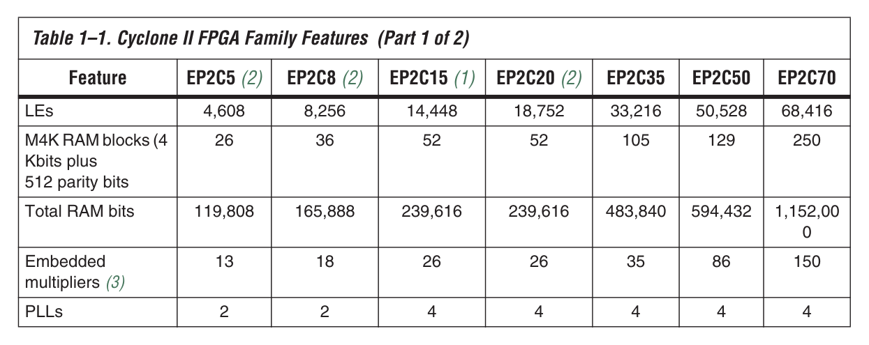
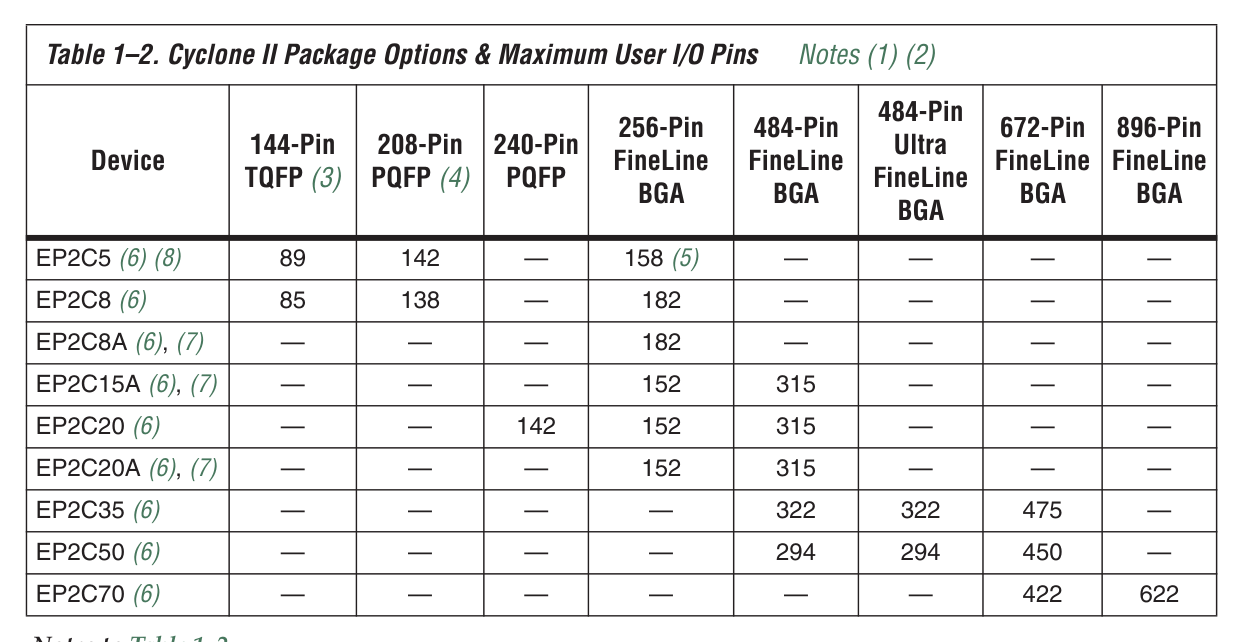
Table 1–1 lists the Cyclone II device family features. Table 1–2 lists the
Cyclone II device package offerings and maximum user I/O pins.
| 1–4 | Altera Corporation |
|---|---|
| Cyclone II Device Handbook, Volume 1 | February 2008 |
(Altera is a trademark and service mark of Altera Corporation in the United States and other countries. Altera products are the intellectual property of Altera Corporation and are protected by copyright laws and one or more U.S. and foreign patents and patent applications.)
Table 1–1. Cyclone II FPGA Family Features (Part 2 of 2)
| Feature | EP2C5 (2) | EP2C8 (2) | EP2C15 (1) | EP2C20 (2) | EP2C35 | EP2C50 | EP2C70 |
|---|---|---|---|---|---|---|---|
| Maximum user | 158 | 182 | 315 | 315 | 475 | 450 | 622 |
I/O pins Notes to Table 1–1:
(1) The EP2C15A is only available with the Fast On feature, which offers a faster POR time. This device is available in
(2) The EP2C5, EP2C8, and EP2C20 optionally support the Fast On feature, which is designated with an “A” in the devices are only available in industrial grade.
(3) This is the total number of 18 × 18 multipliers. For the total number of 9 × 9 multipliers per device, multiply the
| Altera Corporation | 1–5 |
|---|---|
| February 2008 | Cyclone II Device Handbook, Volume 1 |
(Altera is a trademark and service mark of Altera Corporation in the United States and other countries. Altera products are the intellectual property of Altera Corporation and are protected by copyright laws and one or more U.S. and foreign patents and patent applications.)
(1) Cyclone II devices support vertical migration within the same package (for example, you can migrate between the
(2) The Quartus® II software I/O pin counts include four additional pins, TDI, TDO, TMS, and TCK, which are not
| (3) | TQFP: thin quad flat pack. |
|---|---|
| (4) | PQFP: plastic quad flat pack. |
| (5) | Vertical migration is supported between the EP2C5F256 and the EP2C8F256 devices. However, not all of the DQ |
and DQS groups are supported. Vertical migration between the EP2C5 and the EP2C15 in the F256 package is not supported.
(6) The I/O pin counts for the EP2C5, EP2C8, and EP2C15A devices include 8 dedicated clock pins that can be used pins that can be used for data inputs.
(7) EP2C8A, EP2C15A, and EP2C20A have a Fast On feature that has a faster POR time. The EP2C15A is only available
(8) The EP2C5 optionally support the Fast On feature, which is designated with an “A” in the device ordering code. Device Handbook. Cyclone II devices support vertical migration within the same package (for example, you can migrate between the EP2C35, EPC50, and EP2C70 devices in the 672-pin FineLine BGA package). The exception to vertical migration support within the Cyclone II family is noted in Table 1–3.
| 1–6 | Altera Corporation |
|---|---|
| Cyclone II Device Handbook, Volume 1 | February 2008 |
(Altera is a trademark and service mark of Altera Corporation in the United States and other countries. Altera products are the intellectual property of Altera Corporation and are protected by copyright laws and one or more U.S. and foreign patents and patent applications.)
Appendix C Explanation of the IEEE/IEC Standard for Logic Symbols (Dependency Notation)*
The IEEE/IEC standard for logic symbols introduces a method of determining the complete logical operation of a given device just by interpreting the notations on the symbol for the device. At the heart of the standard is dependency notation, which provides a means of denoting the relationship between inputs and outputs without actually showing all of the internal elements and interconnections involved. The information that follows briefly explains the standards publication IEEE Std. 91–1984 and is intended to help in the understanding of these new symbols. A complete explanation of the logic symbols is available from Texas Instruments, Inc., in Publication SDYZ001, “Overview of IEEE Std 91–1984.” They also have a publication (SZZZ003) entitled “Using Functional Logic Symbols,” which explains several applications of the symbols.
Explanation of Logic Symbols
F. A. Mann Texas Instruments Incorporated
Contents
1.0 INTRODUCTION 2.0 SYMBOL COMPOSITION 3.0 QUALIFYING SYMBOLS *Courtesy of Texas Instruments, Inc.
Institute of Electrical and Electronics Engineers, Inc. IEEE Standards Office 345 East 47th Street New York, N.Y. 10017 International Electrotechnical Commission (IEC) publications may be purchased from: American National Standards Institute, Inc. 1430 Broadway New York, N.Y. 10018
Appendix D Answers to Odd-Numbered Problems
Chapter 1 (d) Tanks B and C, temperature high
(e) Tank C, temperature and pressure high
1–1. (a) 610 (b) 1110 (c) 910 (d) 710
1–19. (a) sku43 (b) 534B55343316
(e) 1210 (f) 7510 (g) 5510 (h) 18110
| (i) 16710 | (j) 11810 | ||
|---|---|---|---|
| E1–1. (a) 0000 0101 | (b) Eleven | (c) 0E | (d) 27 |
| 1–3. (a) 318 | (b) 358 | (c) 1348 | (d) 1318 |
(e) 1558
Chapter 2
1–5. (a) 2310 (b) 3110 (c) 1210 (d) 5810
| (e) 4110 | 2–1. (a) 0.5 ms | (b) 2 ms | (c) 0.234 ms | |||
|---|---|---|---|---|---|---|
| 1–7. (a) B916 | (b) DC16 (e) C616 | (c) 7416 (g) 1.33 kHz | (d) FB16 (h) 0.667 MHz | (d) 58.8 ns | (e) 500 kHz | (f) 10 kHz |
| 1–9. (a) 13410 | (b) 24410 (d) 17110 | (c) 14610 (e) 96510 | 2–3. (a) 2.16 ms 2–5. | (b) LOW | ||
| 1–11. (a) 9810 | (b) 6910 | (c) 7410 | (d) 3610 | Cp |
(e) 8110
| Vout1 | 4 V | ||||
|---|---|---|---|---|---|
| 1–13. | 0 V | ||||
| Decimal | Binary | Octal | BCD | Hexadecimal | 4 V |
Vout2
| (a) | 35 | 0010 0011 | 043 | 0011 0101 | 23 | 0 V | |
|---|---|---|---|---|---|---|---|
| (b) | 41 | 0010 1001 | 051 | 0100 0001 | 29 | 8 V | |
| (c) | 43 (d) (e) | 0010 1011 78 58 | 053 0100 1110 0011 1010 | 0100 0011 116 072 2–7. 1–15. (a) 010 0101 (b) 0100100 0110001 0110100 1–17. (a) Tank A, temperature high; tank C, pressure high | 2B 0111 1000 0101 1000 V1 = 0V V2 = 4.3V V3 = 4.3V (c) 1001110 0101101 0110110 (d) 1000011 1010000 1010101 (e) 1010000 1100111 2–11. Cp (b) Tank D, temperature and pressure high | Vout3 4E 3A V5 = 4.3V V6 = 5.0V V7 = 0V V4 = 0.7V 2–9. That diode will conduct raising V7 to 4.3 V (“OR”). 5 V 0 V 3.85 V | 4 V |
Vout
(c) Tanks B and D, pressure high 0 V
| 2–15. Because, when the transistor is turned on | HIGH; otherwise, the output is LOW. |
|---|---|
| (saturated), the collector current will be | (b) The output is HIGH whenever any input |
(IC = 5V>RC)
| excessive | is HIGH; otherwise, the output is LOW. | ||
|---|---|---|---|
| 3–5. (a) | X = ABC | (b) | X = ABCD |
2–17. The totem-pole output replaces RC with a
(c) X = A + B + C
The transistor prevents excessive collector 3–7. A high-level output when turned on.
2–19. (a) 8.0 MHz (b) 125 ns B
2–21. P3 parallel, P2 serial
X 2–23. A HIGH on pin 2 will turn Q1 on, making RESET_B approximately zero.
E2–1. (a) Let (b) 24 A
Cp = 5V>0V,Vout3 = 0V>5V,
E2–3. (a)
B
| inverse of each other | Cp = 5V>0V,Vout3 = 0V>8V |
|---|---|
| (b) | X |
(c) Cp and Vout3 are in phase.
E2–5. (a) V1 = 4.3V,V2 = 0V,V3 = 4.3V,
3–9.
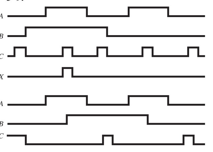
| 1 | 0 | 1 | 0 | X |
|---|---|---|---|---|
| 1 | 1 1 | 0 1 | 0 1 | 1 |
3–11.
(b) A B C D X
| 0 | 0 | 0 | 0 | 0 | B | ||||||||
|---|---|---|---|---|---|---|---|---|---|---|---|---|---|
| 0 | 0 | 0 | 1 | 0 | |||||||||
| 0 | 0 0 0 | 1 0 1 | 0 1 0 | 0 1 0 | X 0 0 | ||||||||
| 0 | 1 | 0 | 1 | 0 | A | ||||||||
| 0 | 1 0 | 1 1 | 0 1 | 0 1 | B 0 | ||||||||
| 1 | 0 1 1 | 0 0 0 | 0 0 1 | 0 1 0 | X 0 0 | ||||||||
| 1 | 0 1 | 1 1 | 1 0 | 0 0 | 3–13. 0 | ||||||||
| 1 | 1 1 | 0 1 | 1 1 | 0 0 | Clock 0 | 1 | 2 | 3 | 4 | 5 | 6 | 7 | 8 |
| 1 | 1 | 1 | 1 | 1 | Enable |
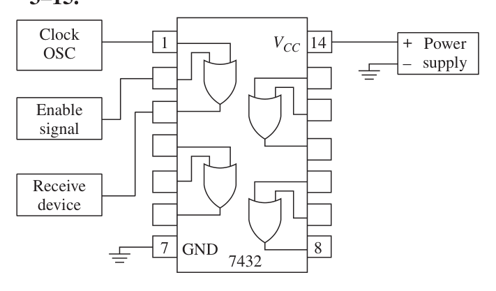
3–17. Two
3–39. U = Cp,A,B W = B,C
3–19. To provide pulses to a digital circuit for
| troubleshooting purposes | V = C,D | X = Cp,C,D |
|---|---|---|
| 3–21. HIGH, to enable the output to change with | 3–41. |
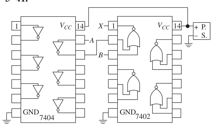
X = 1 3–43. HIGH; to see inverted output pulses
Y = 1 (otherwise, output would always be HIGH). 3–45. There is no problem.
3–31. W = 1
3–47. With all inputs HIGH, pin 8 should be
X = 0 LOW. Next try making each of the 8 inputs Y = 0 LOW, one at a time, while checking for a Z = 0 HIGH at pin 8.
| 3–33. It enables or disables the other inputs. | 3–49. AND-74HC08; U3:A | = | location C2, |
|---|---|---|---|
| 3–35. | U3:B | = | location D2 OR-74HC32; |
location B7
A = LOW (GND), pin 40 HIGH (+5)
B 3–53. Place probe-A on the input of the inverter
C (WATCHDOG_CLK). Using the same of U4:A. Probe-B should display the
X complement of probe-A.
E3–1. (a) X = 1,Y = 1
D (b) X = 0,Y = 0
(c) A B X A B Y
| 0 | 0 | 0 | 0 | 0 | 0 | |
|---|---|---|---|---|---|---|
| F | 0 | 1 | 0 | 0 | 1 | 1 |
| 1 | 0 | 0 | 1 | 0 | 1 |
Y
1 1 1 1 1 1
E3–5. (a) Vcc (b) Logic pulser (c) Logic probe
(d) Ground (e) Vcc C
E3–7. (a) X = 0,Y = 0
| (b) | X = 1,Y = 1 | A | |
|---|---|---|---|
| E3–9. (a) Yes | (b) | X = AB | (c) 6mS |
Chapter 5
E3–11. (a) NAND (b) NOR
E3–13. (a) X = C¿,D¿,Cp (b) Y = BD¿ 5–1. W = (A + B)(C + D)
X = AB + BC E3–15. (a) U1b, U1c, U1d are bad. Y = (AB + B)C (b) U2a, U2c are bad. Z = (AB + B + (B + C))D E3–17. (a) U1b, U1c are bad.
5–3. (a) A
(b) U2a, U2d are bad. B M
Chapter 4 C
D
4–1. The 7400-series uses hard-wired logic. The (b) A
| designer must use a different IC for each | B |
|---|---|
| logic function. Programmable logic | C |
N D contains thousands of logic gates that can (c)
| be custom configured by the designer to | A |
|---|---|
| perform any logic desired. | P |
| 4–3. Hardware Description Language | B |
C
4–5. (a) 3 (b) 5
(d) A B
| from a PC and program the on-board | Q |
|---|---|
| FPGA, which can then be tested with | C |
| actual I/O signals. | D |
| (e) | A |
4–9. The PLA provides programmable OR gates
for combining the product terms. B
4–11. So it will not lose its programmed logic C
| design when power is removed | D |
|---|---|
| (f) | A |
4–13. The look-up table method
4–15. They must be reprogrammed. B
4–17. It translates the information from the C
S design entry stage into a binary file that is D later used to program the CPLD. 4–19. Text
0 0 0 0 0 0 0 0 0 0 0 0 0
0 0 0 1 1 0 0 1 1 0 0 1 0
0 0 1 0 1 0 0 0 0 0 1 0 0
| 0 | 0 | 1 | 1 | 1 | 1 | 0 | 1 | 1 | 0 | 1 | 1 | 1 | ||
|---|---|---|---|---|---|---|---|---|---|---|---|---|---|---|
| X | :OUT bit); | 0 | 1 | 0 | 0 | 0 | 0 | 0 | 0 | 0 | 1 | 0 | 0 | 0 |
| END and3; | 0 | 1 | 0 | 1 | 1 | 1 | 0 | 1 | 1 | 1 | 0 | 1 | 1 | |
| 4–23. | (a) | 0 | 1 | 1 | 0 | 1 | 0 | 0 | 1 | 1 | 1 | 1 | 0 | 0 |
A
| X | 0 | 1 | 1 | 1 | 1 | 1 | 1 | 1 | 1 | 1 | 1 | 1 | 1 |
|---|---|---|---|---|---|---|---|---|---|---|---|---|---|
| 1 | 0 | 0 | 0 | 0 B | 0 1 | 0 0 | 0 0 | 0 1 | 1 | 1 | 0 | 1 | 1 |
C
1 0 1 0 1 0 0 0 1
| A | 1 | 0 | 1 | 1 | 1 | 1 | 0 | 1 | 1 | |
|---|---|---|---|---|---|---|---|---|---|---|
| 1 | 1 | 0 | 0 | 1 | 0 | 0 | 0 | 1 | ||
| B | Y 1 | 1 1 | 1 1 | 0 0 | 1 1 | 1 0 | 1 0 | 0 1 | 1 1 | 1 |
| C | 1 | 1 | 1 | 1 | 1 | 1 | 1 | 1 | 1 |
(c) Distributive law B
5–7. Z
| W = (A + B)BC | D | D | |
|---|---|---|---|
| A | NC | ||
| W = BC | B W | E E | NC |
C Z = ABC + CD
| X = (A + B)(B + C) | A |
|---|---|
| 5–11. | X = (A + B)(D + C) |
| X = B + AC | C |
X
B 5–13. Break the long bar and change the AND to
an OR, or the OR to an AND.
| Y = A + (A + B)BC | A | 5–15. Y and Z are both ORs. |
|---|---|---|
| B | Y |
Y = A + BC 5–17. C B A
Z = AB + B + BC A NC A W W = A+B
| Z = B | B | Z | C | C | NC |
|---|---|---|---|---|---|
| C | NC |
A B
5–9. B
X X = B+C Y
D B D V C A
| V = C(A+D) | A |
|---|---|
| B | C |
C C 5–19. W
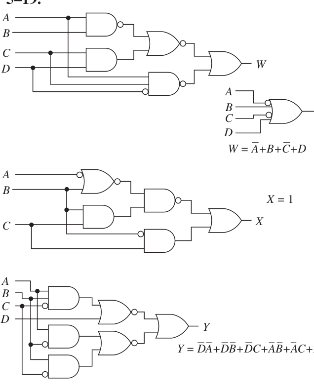
B (b)
D X = A C
Y 5–33. (a)
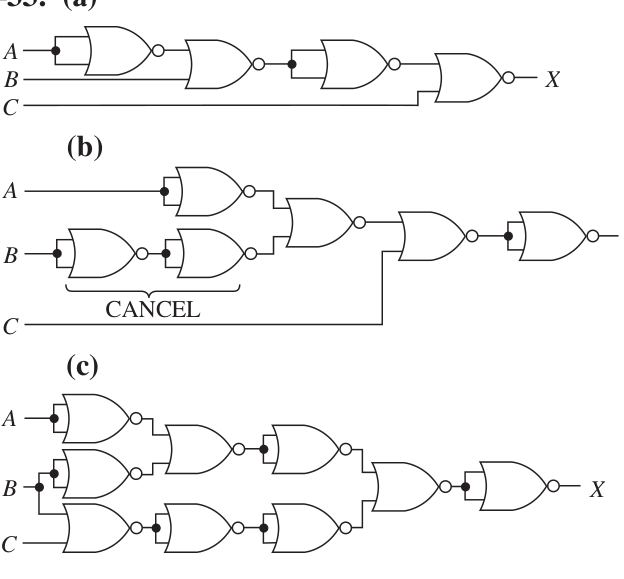
5–35. u. SOP x. SOP
5–23. A v. POS y. POS
| B | w. POS | z. POS, SOP |
|---|---|---|
| C | 5–37. D | X = A + BC Y = B + AC |
Z = AC + AB + ABC
5–25. (23) A
| (22) | ABCD>11 | X = CD + AC + B | Y = 1 |
|---|---|---|---|
| B | 5–39. (a) | (b) |
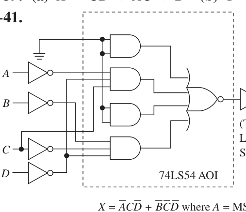
1 0 0 1 1 1
| 1 | 0 | 1 | 0 | 0 1 | ||
|---|---|---|---|---|---|---|
| 1 | 0 | 1 | 1 | 0 0 | pin 9 should be connected to pin 10 (not 9 | |
| 1 | 1 | 0 | 0 | 0 0 | to GND). | |
| 1 | 1 | 0 | 1 | 1 0 | 5–45. | WATCHDOG_EN �Qa |
| 1 | 1 | 1 | 0 | 0 1 | pin6 = P1.0 + A15 |
5–47. (a)
1 1 1 1 1 0
5–29. (c) quad 2 input AND
(a)
| (d) | RD | is LOW or | WR | is LOW |
|---|---|---|---|---|
| (b) | B = KD + HD |
E5–1. (a)
(c) (b) B = D(K + H) (d) (b) X = BC + A
(b) Y = AB + AB �AB = 1
(c) B 6–9. A7 = 101001110
| C | 4C = 010011000 | |
|---|---|---|
| E5–7. | X = AB¿C¿ + A¿BC¿ + AB¿C | 79 = 011110010 |
| E5–9. (a) 2 | F3 = 111100111 | |
| (b) | X = B¿C¿ | 00 = 000000001 |
FF = 111111111 E5–11. (a) 6
| (b) | X = B¿ + C¿ | 6–11. | |||||
|---|---|---|---|---|---|---|---|
| (c) | B | ||||||
| X | 24 | 23 | 22 | 21 | 20 | 23222120 | 24 |
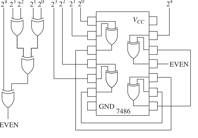
(b) Gate 2
(c) 6–13.
A TRANSMISSION
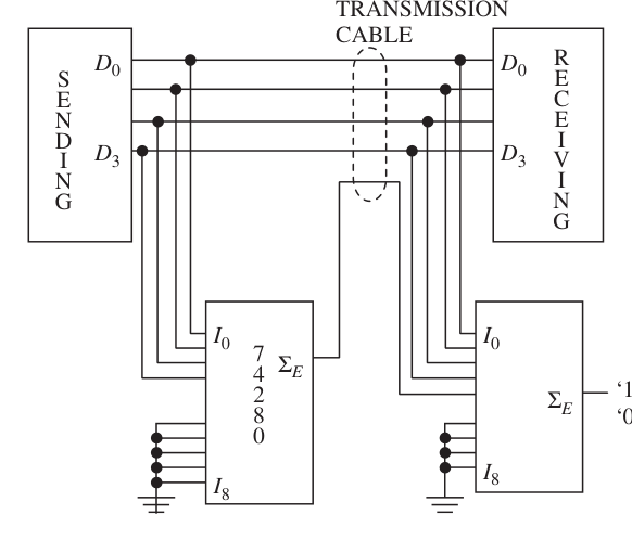
B 6–15. Yes; LOW
| X | Ex-OR | 6–17. |
|---|---|---|
| Y | Ex-NOR | X0 |
A8 A12 6–5. X1
| “AND” | A9 | |
|---|---|---|
| A13 | X4 | |
| A | X2 | P3.4 |
A10 A14 Ex-OR X3 A11
B A15
| (b) | (f) 162 | (g) AB45 | (h) A000 | ||||
|---|---|---|---|---|---|---|---|
| (c) | A | B | X | A | B | Y | 7–13. 2CF0H |
7–15. b, c, e
| 0 | 0 | 0 | 0 | 0 | 1 | |
|---|---|---|---|---|---|---|
| 0 | 1 | 1 | 0 | 1 | 0 | 7–17. For the LSB addition of two binary num- |
| 1 | 0 | 1 | 1 | 0 | 0 | bers |
| 1 | 1 | 0 | 1 | 1 | 1 | ©o = OK |
7–19. Co = NO
E6–3. (a) Yes, because it is an Ex-OR. 7–21.
| A3 B3 | A2 B2 | A1 B1 | A0 B0 | |||||||||
|---|---|---|---|---|---|---|---|---|---|---|---|---|
| E6–5. | X = (A¿B + AB¿)BC = A¿BC | |||||||||||
| E6–7. Because they both have an odd number of 1s. | A | B | Ci | A | B | Ci | A | B | Ci | A | B | Ci |
| FA | FA | FA | FA | |||||||||
| Co | Σ | Co | Σ | Co | Σ | Co | Σ |
Chapter 7
| Σ4 | Σ3 | Σ2 | Σ1 | Σ0 | |||||||||
|---|---|---|---|---|---|---|---|---|---|---|---|---|---|
| 7–1. (a) 1001 | (b) 1111 0010 | (c) 1 1100 (d) 100 0010 (g) 10100 1111 7–3. (a) 1 0101 | (e) 1100 1000 (h) 10110 0000 (b) 10 1010 (d) 1 0001 0001 | (f) 10010 7–23. (c) 11 1100 (e) 1 1110 1100 0011 | |||||||||
| NC | NC | A5 | B5 (f) 111 0111 0001 | A4 (g) 1 1001 0011 | B4 | A3 | B3 | A2 | B2 | A1 | B1 | A0 | B0 |
(h) 111 1110 1000 0001
| A4 | B4 | A3 | B3 | A2 | B2 | A1 | B1 | A4 | B4 | A3 | B3 | A2 | B2 | A1 | B1 | ||
|---|---|---|---|---|---|---|---|---|---|---|---|---|---|---|---|---|---|
| 7–5. | +15 | 0000 1111 | -1 | 1111 1111 +14 +12 | NC 0000 1110 0000 1100 | Cout -2 -4 | Cin 1111 1110 1111 1100 | Cout Σ4 NC | Cin Σ3 Σ6 | 7483 Σ2 Σ5 | 7483 Σ1 Σ4 +9 | Σ4 +13 Σ3 +11 +10 0000 1001 +8 | Σ3 0000 1101 Σ2 0000 1011 0000 1010 -7 0000 1000 | Σ2 -3 Σ1 -5 -6 1111 1001 -8 | Σ1 1111 1101 Σ0 1111 1011 1111 1010 7–25. 1111 1000 | ||
| +7 | -9 | A7 | B7 | A6 | B6 | A5 | B5 | A4 | B4 | A3 | B3 | A2 | B2 | A1 | B1 | A0 | B0 |
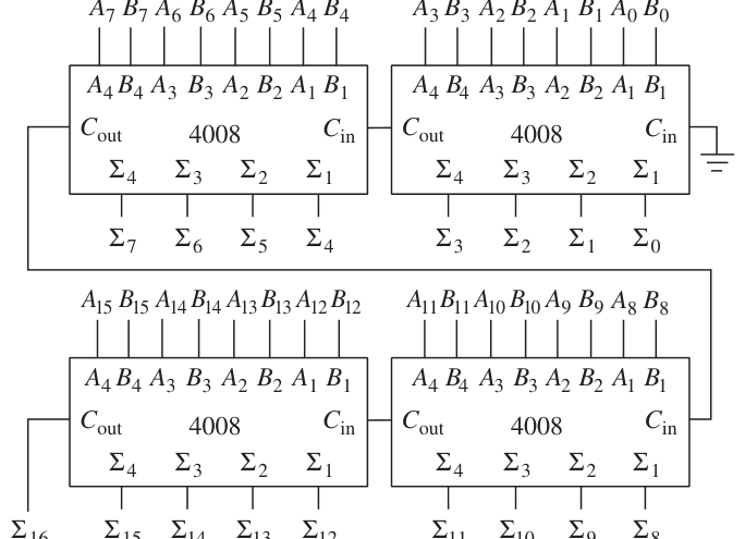
| (f) | 10000001 = -127 | |
|---|---|---|
| (g) | 01111111 = +127 | |
| (h) | 11111111 = -1 | 7–27. The Ex-OR gate third from right is bad. |
Also, the full-adder fourth from right is
7–9. (a) 0000 1100 (b) 0000 0110
bad.
| (c) 0011 0010 | (d) 0000 1110 | ||
|---|---|---|---|
| 7–29. | S3 - S0 = 0100 | ||
| (e) 0000 1010 | (f) 0011 1011 | ||
| (g) 1111 0100 | (h) 1010 1100 | (a) 1110 | (b) 0001 |
+5 A7•• A0 A4 77 2D FF 1D
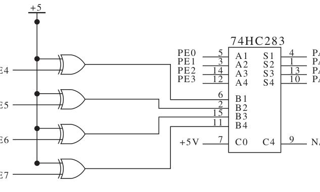
order A = B
(b) Full adder TT A > B The number of HIGH inputs is two or
| more. | 23222120 | |||||||||||||
|---|---|---|---|---|---|---|---|---|---|---|---|---|---|---|
| 8–5. | 0 | 1 | 2 | 3 | 4 | 5 | 6 | 7 | 8 | 9 | ||||
| E7–3. (a) 0011 1011 | (b) 0111 0000 | |||||||||||||
| 10011(1 = ON) | 10111(1 = ON) | 0 | 0 | 0 | 0 | 0 | 1 | 1 | 1 | 1 1 | 1 | 1 | 1 | 1 |
| E7–5. (a) | (b) | |||||||||||||
| 0 | 0 | 0 | 1 | 1 | 0 | 1 | 1 | 1 1 | 1 | 1 | 1 | 1 | ||
| 0 | 0 | 1 | 0 | 1 | 1 | 0 | 1 | 1 1 | 1 | 1 | 1 | 1 | ||
| Chapter 8 | 0 | 0 | 1 | 1 | 1 | 1 | 1 | 0 | 1 1 | 1 | 1 | 1 | 1 | |
| 0 | 1 | 0 | 0 | 1 | 1 | 1 | 1 | 0 1 | 1 | 1 | 1 | 1 | ||
| 8–1. (a) See top numbers. | 0 | 1 | 0 | 1 | 1 | 1 | 1 | 1 | 1 0 | 1 | 1 | 1 | 1 | |
| 0 | 1 | 1 | 0 | 1 | 1 | 1 | 1 | 1 1 | 0 | 1 | 1 | 1 |
(b) See lower numbers.
| 0 | 1 | 1 | 1 | 1 | 1 | 1 | 1 | 1 1 | 1 | 0 | 1 | 1 | ||
|---|---|---|---|---|---|---|---|---|---|---|---|---|---|---|
| 1 | 0 | 0 | 0 | 1 | 1 A7B7 | 1 A6B6 | 1 A5B5 | 1 1 A4B4 | 1 A3B3 | 1 A2B2 | 0 A1B1 | 1 A0B0 | ||
| 1 | 0 | 0 | 1 | 1 | 1 1 1 | 1 1 1 | 1 0 0 | 1 1 1 1 | 1 1 1 | 1 0 0 | 1 0 0 | 0 1 1 | ||
| 1 | 0 | 1 | 0 | 0 | 1 | 1 | 1 | 1 | 0 | 0 | 0 | 0 | 1 | 1 1 |
8–7. Active LOW outputs are 0 when selected.
| 0 1 | 0 | 0 | 0 | 0 | 0 | 0 | 0 | 0 | Active HIGH outputs are 1 when selected. |
|---|---|---|---|---|---|---|---|---|---|
| 1 | 1 | 0 | 1 | 0 | 1 | 8–9. 1 | Time OUT = 1 if A=B | Low Output Interval t0-t1 t1-t2 t2-t3 t3-t4 t4-t5 | Pulse At: None (E3 disabled) None (E3 disabled) 5 4 3 |
8–3. (a)
t5-t6 2
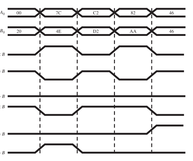
(b) 0, 1, 0, 1, 1 EI 8–29. (a) The 74150 is not working. The data select is set for input D7, which is 0. I3
| Therefore, | Y | should be 1 but it is not. |
|---|---|---|
| I4 | (b) The 74151 is OK. The data select is set |
for input I0, which is 1. Y should equal
1 and Y should equal 0, which they do. (c) The 74139 has two bad decoders.
A1 Decoder A is enabled and should outA2 disabled and should output 1111 but EO does not. (d) The 74154 is OK. The chip is disabled,
GS so all outputs should be HIGH, which 8–17. 8–31. (a) Write to memory bank 5, location 3H.
| 0 | 1 | 2 | 3 | 4 | 5 | 6 | 7 | 8 | 9 | 10 | 11 | 12 | 13 | 14 | 15 | (b) Read from memory bank 6, location |
|---|---|---|---|---|---|---|---|---|---|---|---|---|---|---|---|---|
| 1 | 1 | 1 | 1 | 1 | 1 | 1 | 1 | 1 | 1 | 1 | 1 | 0 | 1 | 1 | 1 |
C7H.
1 1 1 1 1 1 0 1 1 1 1 1 1 1 1 1
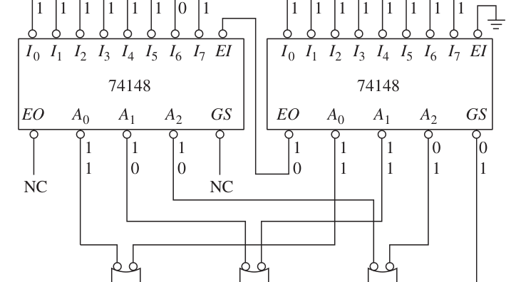
| AD13 | 0 | 0 | ||||
|---|---|---|---|---|---|---|
| 1 | 1 | 0 | 0 | AD14 | 0 | 0 |
| 1 | 0 | 0 | 1 | AD15 | 0 | 0 |
| 20 | 21 | 22 | 23 | AS | 0 | 0 |
| 8–19. (a) 1000002 | (b) 1011102 | (c) 1101112 |
(d) 10001002
8–41. 74151
8–21. See #20 (lower numbers). 4 I0 Z 5
| PD | PD5 | ||||
|---|---|---|---|---|---|
| 10102 = 1111 | 11112 = 1000 | TD | 3 | I1 | |
| 8–23. (a) | (b) | 2 | 6 | ||
| PC | I2 | Z | N/C | ||
| (c) | 00112 = 0010 | (d) | 00012 = 0001 | 1 | I3 |
TC
| PB | 15 | I4 | |||
|---|---|---|---|---|---|
| 8–25. | A | To S0’s | TB | 14 | I5 |
| B | To S1’s | PA | 13 | I6 | |
| Data | TA C | 12 To S2’s | I7 | ||
| Select | D PD2 | 11 A | |||
| To E0 | (Low-order E | 10 PD3 | B | ||
| multiplexer) | PD4 7 | 9 E | C |
To E1 To E2
E8–1. (a) A0 to A3 = B0 to B3
To E3 (b) NOR
Y0 Y1
Y2 Data out
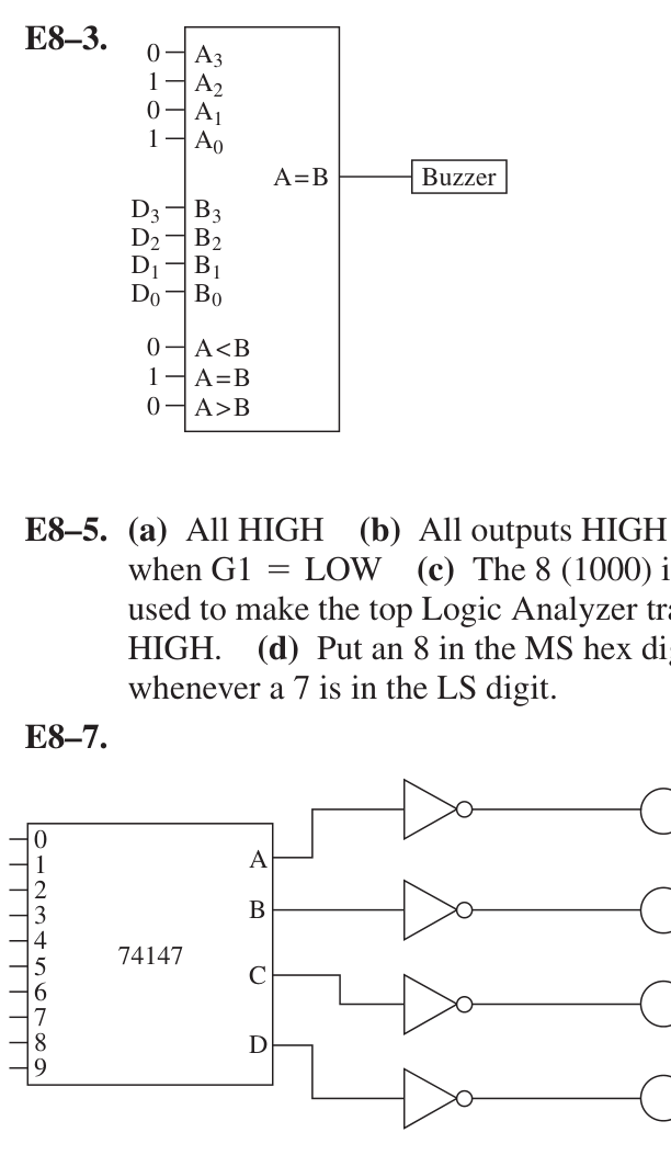
9–11. 7400:PD = 75mW(max)
E8–9. (a) 00 (b) 11 74LS00:PD = 15mW(max)
| E8–11. (a) Switch S1 has no effect on flashing | 9–13. (a) 7400: HIGH state | (minlevels) = 0.4V |
|---|---|---|
| speed. | LOW state | (maxlevels) = 0.4V |
| (b) Vcc at S1 is open. | 74LS00: HIGH state LOW state | (minlevels) = 0.7V (maxlevels) = 0.3V |
E8–13. (a) LED2
| (b) SWC | (b) The 74LS00 has a wider margin for |
|---|---|
| (c) SWG | the HIGH state. The 7400 has a wider |
| (d) 74LS138 | margin for the LOW state. |
| E8–15. (a) SWA | 9–15. The open-collector FLOAT level is made a |
| (b) SWG | HIGH level by using a pull-up resistor. |
| (c) V0 | 9–17. The 7400 series is faster than the 4000B |
| (d) 74151 | series but dissipates more power. |
9–19. Because MOS ICs are prone to electro-
static burnout.
Chapter 9
9–21. Where speed is most important, ECL is
| 9–1. D1 and D2 provide some protection against | faster but uses more power. | |
|---|---|---|
| negative input voltages. | 9–23. The 74HC family | |
| 9–3. From Figure 9–2(a), there is �0.2 V | 9–25. Interfacing (c) and (e) will require a pull- | |
| dropped across the 1.6 k, 0.7 V across | up resistor to “pull up” the TTL HIGH- | |
| VBE3, | and 0.7 V across D3, leaving �3.4 V | level output to meet the minimum |
| at the output terminal. | HIGH-level input specifications of the | |
| 9–5. Negative sign signifies current leaving the | CMOS gates. | |
| input or output of the gate. | 9–27. (a) 10 | (b) 400 |
100 nS G D
| CLK | Q |
|---|---|
| 22 nS | 15 nS |
10–11.
E9–1. (a) HIGH (b) ON, OFF (c) OFF, ON
E
E9–3. (a) 12 ns, 12 ns (b) 6.3 ns, 11 ns
C9–1. (a) 4 mA to 24 mA (b) 2 mA to 8 mA
D C9–3. (a) 1.7 V, 0.7 V, 2.0 V, 0.4 V
(b) 1.17 V, 0.630 V, 1.35 V, 0.45 V Q
Chapter 10
10–15.
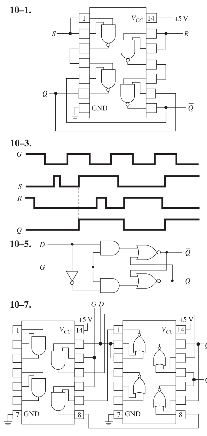
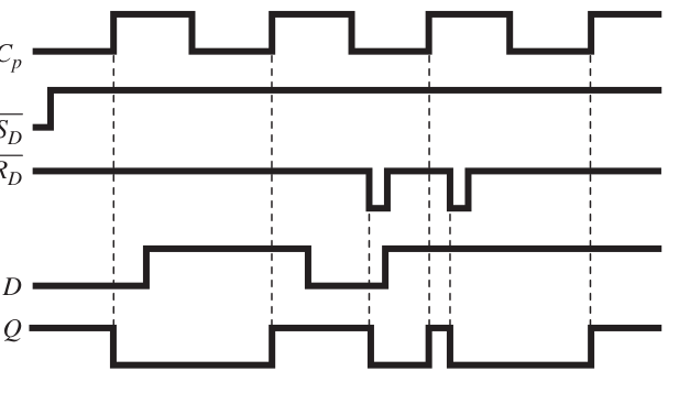
10–17. The 7474 is edge-triggered; the 7475 is
pulse-triggered. The 7474 has asynchro-
| 10–3. | nous inputs at | SD | and | RD. |
|---|---|---|---|---|
| G | 10–19. The triangle indicates that it is an edge- |
triggered device as opposed to being pulsetriggered. S 10–21. R
1 VCC 14 +5 V CP
10–5. D
Q G Q
10–7. G D
| 7 | GND | 8 | CP′ | ||
|---|---|---|---|---|---|
| +5 V | +5 V | ||||
| 1 | VCC | 14 | 1 | VCC | 14 |
10–23. The toggle mode
Q 10–25. The 7476 accepts J and K data during the entire positive level of CP, whereas the 74LS76 only looks at J and K at the negaQ tive edge of CP.
7 GND 8 7 GND 8
| Trigger | CP |
|---|---|
| SD | D |
RD Sd′
J Rd′ Q Q1
E10–7. (a) J = 0,K = 1, pulse Cp¿ LOW then
Q2 HIGH
| (b) | J = 1,K = 0, | pulse | Cp¿ | LOW then |
|---|---|---|---|---|
| 10–29. | HIGH | (c) Q toggles each time | Cp¿ CP | goes LOW (d) Q stuck HIGH |
(e) Set: Pulse S LOW then HIGH; Reset:
SD Pulse R LOW then HIGH Data
Q Cp′
10–31. K
CP Sd′ Q SD Q
Chapter 11
10–33. The ¿373 is a transparent latch. If the tim- 11–1. RD will pass through to Q while E is HIGH Cp and latch on to the data when E goes LOW.
| As long as the positive timing pulses are | K | |
|---|---|---|
| very narrow ( | 6 | 10 ms), the display will not |
Q
flicker. The ¿273 is the preferred device,
11–3. ta = 20ns td = 30ns
10–35. (a) HIGH (b) no (c) Qa must go tb = 30ns te = 20ns
HIGH while WATCHDOG_EN is HIGH. tc = 20ns tf = 30ns 11–5. Proper circuit operation depends on tp of HIGH.)
the 7432 being �10ns. The worst-case tp is specified as 15 ns, but the actual tp may
E10–1. (a) 1, 0 be less. If it’s actually less than 10 ns, the
(b) 0, 1 circuit won’t operate properly. E10–3. (a) Top inverter (b) Vcc (c) None (d) R switch
Rlim RD
| 35 ns | 330 |
|---|---|
| CLOCK | Q1 |
J, K Q2 25 ns
| CpD | Q3 |
|---|---|
| Q | Q4 |
Q5
11–9. Q6
Q7
3.6 V Q8 0.2 V
0.7 V 1.9 V 11–25. The switches of U12 and the pull-up resis-
Vin tors are used to place either a HIGH or place a HIGH on one of these lines, the
11–11. corresponding switch must be open. A
closed switch pulls the line to ground. 2.4 V
E11–1. Vt += 1.6V, Vt -= 1.3V
1.7 V
Vin 0.9 V 0.4 V 3.4 V 0V
Vout 1.3V 1.6V
E11–3. (a) Vt += 1.3V, Vt -= 0.83V
tHI = 1.8 volts change Voh = 5V,Vol = 0V tLOW = 2.2 volts change DC = 45% +5V 11–13. It is caused by switch bounce. If the switch
bounces an even number of times, the LED 0V will be off. A debounce circuit would
| correct the problem. | (b) Yes | |
|---|---|---|
| 11–15. Check the output of the 7805 for | +5V | dc. |
Check the fuse. If the fuse is OK, you should check for approximately 12.6 V ac
at the transformer secondary and 20 V dc Chapter 12
+ >-
at the output of the diode bridge and the input to the 7805. sequence of digital states triggered by a
11–17. Light: VA = 0.0495V
timing pulse or clock. Combination logic
Dark: VA = 4.55V
| 11–19. The 7474 can sink 16 mA. Connect the | based on the levels placed at its inputs. | |
|---|---|---|
| positive lead of the buzzer to | +5V | and the |
| negative lead to | Q. | When Q is HIGH, the |
| buzzer is energized via the LOW | Q | output. |
11–21. Icoil = 240mA
| Cp | 0 | 1 | 2 | 3 | 4 | 5 | 6 | 1 | 20 | 1 | 21 | 1 | 22 |
|---|---|---|---|---|---|---|---|---|---|---|---|---|---|
| 1 | J | SD | Q | 1 | J | SD | Q | 1 | J | SD | Q |
RD Cp0
1 K RD 1 K RD 1 K RD D Q 12–19. Q
1 20 1 21 1 22 1 23
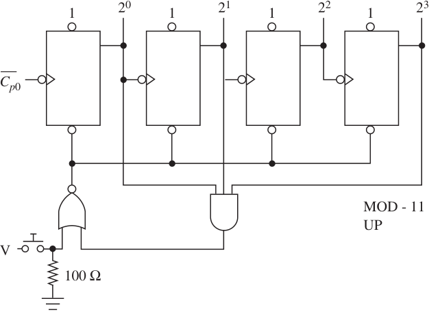
12–21. Q
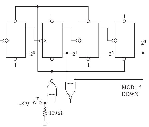
12–13. (a) 2 (b) 4 (c) 4 (d) 5 12–23. +5 V to RD
| Cp | 10 kΩ |
|---|---|
| 20 | 22 |
12–25. Yes, it will work. The inputs to the AND
22 are normally 1–1 until the push button is If either AND input goes LOW, its output goes LOW, resetting the counter. This is
| because the | draws less current than | |||
|---|---|---|---|---|
| the | 100@� | resistor when the push button | CPU | |
| 0 | 1 | 2 | 3 | 4 |
| is depressed. | CPD | |||
| 0 | 1 | 2 | 3 | 4 |
12–27. PL
Output TCU
| Cp1Q0Q1Q2Q3 | Cp1Q0Q1Q2Q3 | TCD | |
|---|---|---|---|
| 7490 | 7492 | NC | |
| Input | Cp0 ÷2 | Cp0 ÷12 | Q0 |
Q1
12–29. Q2
| 60pps | 7492 | 10 pps | 7490 | 1 pps | 7492 | 10 ppm | 7490 | 1 ppm | Q3 | ||||||||
|---|---|---|---|---|---|---|---|---|---|---|---|---|---|---|---|---|---|
| ÷6 | ÷10 | (60 | ÷6 | ÷10 | 5 | 6 | 7 | 8 | 9 | 0 | 5 | 4 | 3 | 2 | 1 | 0 | 9 |
Input
ppm) (60 pph)
| 7492 | 10 pph | 7490 | 1 pph | 7492 | 2 ppd | 7490 | 1ppd |
|---|---|---|---|---|---|---|---|
| ÷6 | ÷10 | (24 | ÷12 ppd) | ÷2 1 | Output 1 | 0 | 1 |
PL an 1110 when
PL D0 D1 D2 D3
12–31. CpU CpU TCU
74193
| NC 202122 | NC | CpD | TCD | NC |
|---|---|---|---|---|
| MR Q0 Q1 Q2 Q3 | Take ÷4 output | Cp1Q0Q1Q2Q3 | from Q2 or TCU |
100 Hz
| 7493 | +5 V | |
|---|---|---|
| NC | Cp0 MR1 | Output |
| MR2 | 330 Ω |
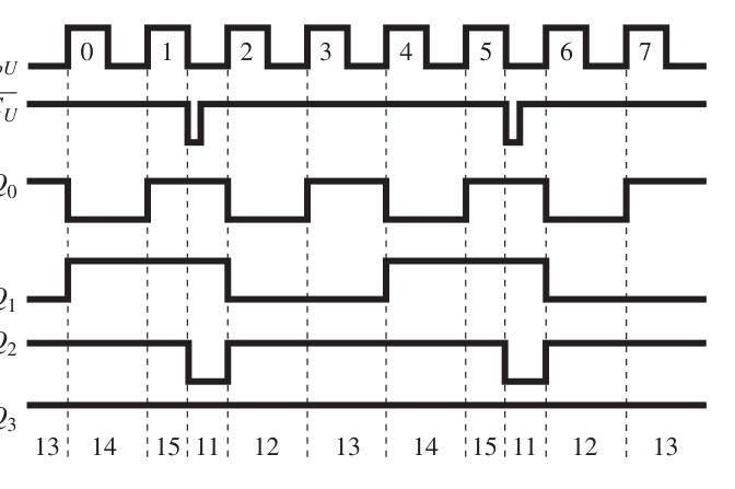
12–37. 12–43. (a) HIGH-order U10, LOW-order U9
| (b) No | (c) By a LOW at the output of | |||||||||
|---|---|---|---|---|---|---|---|---|---|---|
| 0 | 1 | 2 | 3 | 4 | 5 | 6 | 7 | 8 | 9 | U3:B |
CP 12–45.
| 74LS193 | 74151 | (CLK OUT) TO | ||||||
|---|---|---|---|---|---|---|---|---|
| 15 | P0 | Q0 | 3 | 4 | I0 | Z | 5 | PINS 6 & 10 |
| 21 | 1 | P1 | QB | 2 | 3 | I1 | 6 | OF M1 |
| 10 | P2 | QC | 6 | 2 | I2 | Z | N/C | |
| 9 | P3 | QD | 7 | 1 | I3 | |||
| 5 | 12 | 15 | I4 | |||||
| E (CLK IN) | 4 | CU | TCU | N/C | 14 | I5 | ||
| 22 | CD | TCD | 13 | N/C | 13 | I6 | ||
| +5 | 11 | PL | 12 | I7 | ||||
| 14 | MR | 11 | ||||||
| FREQUENCY | 10 | A | ||||||
| SELECT | 9 7 | B C |
E
E12–3. Doesn’t count past 7. Bad MS flip-flop
| Q0 | Q0 | Q2 | ||
|---|---|---|---|---|
| E12–5. (a) Mod-10 | (b) Connect NAND inputs | X | X | Z |
| Q1 | Q2 to 2^3 and 2^2. E12–7. (a) Build a circuit similar to Figure 12–35. (b) Use a third 7490 as div-by-10 with 10 | Q3 (c) 2^2 13–17. Put a switch in series with the phototransis- tor’s collector. With the switch open, the | ||
| pps driving its | CP0¿. 7490 is 1 pps.) Make the input to your 00 to 99 counter switch between those two clock speeds. Cp¿ gate before the first | (The output of that ing nighttime conditions, causing the yellow light to flash, day or night. (c) Place an AND 13–19. input. Disable | input to inverter 1 will be HIGH, simulat- |
it with a NAND gate that outputs a
Cp 0 1 2 3 4 5 6 7 8 9 MR E12–9. S0 S1 MR PL Q0 Cpu
Cpd Q1 Qa
| Qb | Q3 | |||||||||
|---|---|---|---|---|---|---|---|---|---|---|
| Mode | L | L | L | L | RR | R | O | L | R | R |
Qc L
Qd D 13–21. Tcu'
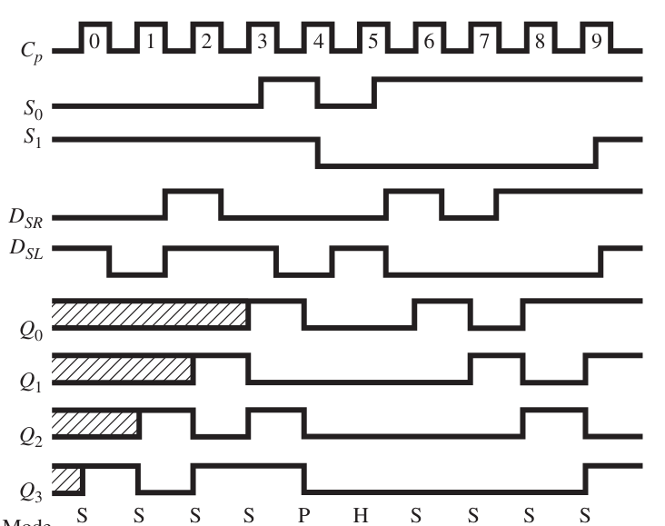
L D 13–13.
Cp 0 1 2 3 4 5 6
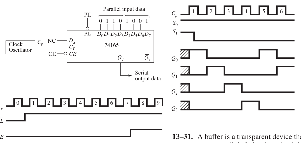
MSB LSB allows data to flow in only one direction; a 13–25. The 74164 is a serial-in, parallel-out, transceiver is bidirectional. whereas the 74165 is a serial- or parallel-
| in, serial-out, shift register. The 74165 pro- | 13–33. (a) U4, U12 | (b) U5, U30, U31, U32, | |||
|---|---|---|---|---|---|
| vides a clock-enable input, | CE. input to the 74164 is the logical AND of | The serial U33 | U36, U37, U38 | (c) U3, U6 | (d) U11, |
| two data inputs (Dsa | � | Dsb). | 13–35. To load | IA0-IA7 | of U30, valid data must |
| be placed on | BD0-BD7 13–27. | by U33, then a LOW to HIGH pulse must be applied to |
the CLK input of U30. When pin 3 of
Serial in U13:A is LOW, a HIGH will appear at LE of U33. This allows the valid data at D0–D7
| DSR | D0 | D1 D2 D3 | DSL | DSR | D0 | D1 D2 D3 | DSL | to pass through to | BD0-BD7. | Next, pin 3 |
|---|---|---|---|---|---|---|---|---|---|---|
| S0 | S0 | S0 | S0 | of U13:A goes HIGH, making LE LOW, | 74194 | NC | NC S1 | 74194 S1 | S1 | S1 |
which causes the data outputs of U33 to re-
| CP | CP | CP | CP | |||||
|---|---|---|---|---|---|---|---|---|
| MR | Q0 | Q1 | Q2 Q3 | MR | Q0 | Q1 | Q2 Q3 | main latched. The HIGH at pin 3 of U13:A |
also enables the decoder U23. Just before
1 1
Serial out OE 1–0–1 to provide an active output at /IOADDR. This is the clock input for U30,
| CP | which passes the valid data at | BD0-BD7 | of | ||||||||||||
|---|---|---|---|---|---|---|---|---|---|---|---|---|---|---|---|
| 0 | 1 | 2 | 3 | 4 | 5 | 6 | 7 | 8 | 9 | 10 | 11 | 12 | 13 | 14 | 15 |
| S0 | U30 out to | IA0-IA7. SHIFT RIGHT | To load SHIFT LEFT | ID0-ID7 | of |
U32, the same process is followed, except
| S1 | A0–A1–A2 are made 0–1–1 before pin 3 of | ||||||||
|---|---|---|---|---|---|---|---|---|---|
| SERIAL | 0 | 0 | 1 | 0 | 1 | 1 | 0 | 1 | DONT CARE |
| IN | U13:A is made HIGH. |
OE
E13–1. (a) 3 (b) R, S, C, S, C, S, C, S
SERIAL FLOAT 1 0 1 1 0 1 0 0 (b) Q^0 Q^1 Q^2 Q^3
| Set S | 1, press C; Set S | 0, press C; | than | 150ms, | let’s say, | 170ms. | That way, if |
|---|---|---|---|---|---|---|---|
| Set S | = | 1, press C; Set S Set S | = = Set S | 1, press C; 0, press C; Set S = | a pulse is missing after = 1, press C; Set S | 170ms 0, press C; = | (the O.S. is not retriggered), the output will go LOW. 0, press C. |
VCC
Chapter 14 Rx 12.9 kΩ
Cx = 0.047 μF
14–1. (a) Monostable (b) Bistable
(c) Astable Output
14–3. 75.6ms NPRO
T
14–5. 32.6ms 1
14–7. Because a Schmitt device has two distinct 1
| switching thresholds, VT+ and VT-; a regu- | 74123 |
|---|---|
| lar inverter does not. The capacitor voltage | Pick Cx = 0.047 μF; Rx = 12.9 kΩ |
charges and discharges between those two
| levels. | 14–15. | |||
|---|---|---|---|---|
| 0 | 0.5 | 1.0 | 1.5 | 2.0 time |
| 14–9. | (μs) | |||
| 3.3 V | A1 |
VC
2.0 V B
6 V Q1 Q2
0 V tw1 = 0.20 μs tHI = 126 μs tLO = 160 μs
DC = 44.1% f = 3.5 kHz 14–17. @0�,f = 89.0kHz
DC = 71.0%
14–11. @10k�,f = 39.8kHz
DC = 59.4%
| Vin | 3 μs | 7 μs | |
|---|---|---|---|
| Vout | 5 μs | 5 μs | 14–19. |
VCC VCC
| RA | 2618 Ω | ||
|---|---|---|---|
| Rx | 7.21 kΩ | ||
| 7 | 8 | 4 | |
| Cx = 0.001 μF | RB | 5236 Ω | 2 |
| 6 | 3 | Vout | |
| .0022 μF | 1 | 5 |
C Vout T .01 μF Vin 74121 Pick Cx = 0.001 μF; Rx = 7.21 kΩ
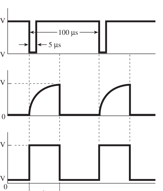
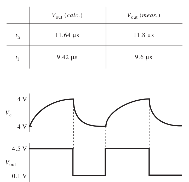
14–23. Chapter 15
VCC 15–1. Converts physical quantities into electrical quantities
8.5K 15–3. Very high input impedance, very high volt-
74LS123
15 RCext age gain, and very low output impedance
| .05�f | 15–5. The | (-) | input is at 0-V potential. | |||
|---|---|---|---|---|---|---|
| 14 | Cext | 15–7. (a) | 20k�,40k�,80k� | |||
| 1 | A | Q | 13 | N/C | ||
| 2 | (b) | D3 DAV IN | D2 B | D1 | D0 | Vout |
| +5 | 3 | CLR | Q | 4 | P1.7 OF U8 | |
| 0 | 0 | 0 | 0 | 0.00 | ||
| 0 | 0 E14–1. (a) | 0 Tcalc = 693mS, | 1 Tmeas = 700mS | -1.25 | ||
| 0 | 0 | 1 (b) | 0 DCVtrig = 20%,DCVout = 70% | -2.50 | ||
| 0 | 0 | 1 (c) | 1 Rext = 722� | -3.75 | ||
| 0 | 1 | 0 | 0 | -5.00 |
Ttrigger:Ttot = 1>10kHz = 100
E14–3. mS, 0 1 0 1 -6.25
| Thi = 70mS | 0 | 1 | 1 | 0 | -7.50 |
|---|---|---|---|---|---|
| Tout:50% * 100mS = 50mS, | 0 | 1 | 1 | 1 | -8.75 |
| 50mS = .693Rext * Cext, | 1 | 0 | 0 | 0 | -10.00 |
| PickCext = .01mf,Rext = 7220�. | 1 1 | 0 0 | 0 1 | 1 0 | -11.25 -12.50 |
| Use those components in a circuit similar | 1 | 0 | 1 | 1 | -13.75 |
| to that in Section 14–5b. | 1 1 1 1 | 1 1 1 1 | 0 0 1 1 | 0 1 0 1 | -15.00 -16.25 -17.50 -18.75 |
15–9. All values of Vout would become positive.
| -2.00 | It then issues | CS1,RD1 | to transfer the con- | |||||||
|---|---|---|---|---|---|---|---|---|---|---|
| 0 | 0 | 0 | 0 | 0.00 | 1 | 0 | 0 | 0 | ||
| -0.25 | -2.25 | verted data to the data bus, then | CS2,WR2, | |||||||
| 0 | 0 | 0 | 1 | 1 | 0 | 0 | 1 | |||
| 0 | 0 | 1 | 0 | -0.50 | 1 | 0 | 1 | 0 | -2.50 | to transfer the data to RAM. |
| 0 | 0 | 1 | 1 | -0.75 | 1 | 0 | 1 | 1 | -2.75 | 15–33. 2.439 to 2.564 V |
| 0 | 1 | 0 | 0 | -1.00 | 1 | 1 | 0 | 0 | -3.00 |
15–35. 9.60 kg
| 0 | 1 | 0 | 1 | -1.25 | 1 | 1 | 0 | 1 | -3.25 |
|---|---|---|---|---|---|---|---|---|---|
| 0 | 1 | 1 | 0 | -1.50 | 1 | 1 | 1 | 0 | -3.50 |
15–37.
0 1 1 1 -1.75 1 1 1 1 -3.75
| 20 | ADC0801–1 | |||||
|---|---|---|---|---|---|---|
| 15–13. To convert the analog output current (Iout) | 7 | Vin (–) | 1sbDB0 | 18 | P1.0 | |
| VccREF | DB1 | 17 | P1.1 | |||
| of the MC1408 to a voltage | ANALOG IN | 6 | Vin (+) | DB2 | 16 | P1.2 |
| DB3 | 15 | P1.3 | ||||
| 8 | DB4 | 14 | P1.4 | |||
| A–GND | DB5 | 13 | P1.5 | |||
| 15–15. (a) 2.5 V | (b) 2.11 V | (c) 1.25 V | DB6 | 12 | P1.6 | |
| msbDB7 | 11 | P1.7 | ||||
| (d) 1.17 V | 9 | Vref/2 | 5 | |||
| N/C | INTR | |||||
| 10K | 19 | 1 | ||||
| VREF = 7.5V. | CLK–R | CS | 2 | |||
| 15–17. By making | The range of Iout | 4 | RD | 3 | ||
| CLK–IN | WR | |||||
| would then be 0 to 1.5 mA. The range of | + | 150 pf |
Vout would be 0 to 7.47 V.
15–19. P2.0
VCC
| 20 | ADC0801–2 | |||||
|---|---|---|---|---|---|---|
| 000 | 7 | Vin (–) | 1sbDB0 | 18 | ||
| VccREF | DB1 | 17 | VCC | |||
| 001 | ANALOG IN | 6 | Vin (+) | DB2 | 16 | |
| DB3 | 15 | |||||
| 3-Bit | 8 | DB4 | 14 | R3 | ||
| 010 | A–GND | DB5 | 13 | 10x | ||
| DB6 | 12 | 11 | ||||
| digital | 9 | msbDB7 | ||||
| 011 | N/C | Vref/2 | 5 | 2 | 1 | |
| output | 10K | INTR | ||||
| 100 | 19 | CLK–R | CS | 1 | 7417 | C1 |
| (ACTIVE- | RD | 2 | .001 | |||
| 4 | CLK–IN | WR | 3 | OC BUFFER | ||
| LOW) | 101 | + |
150 pf
| 0 | 1 | 2 | 3 | 4 | 5 | 6 | 7 | 8 |
|---|---|---|---|---|---|---|---|---|
| E15–1. (a) | D0 = -1V,D1 = -2V, |
Analog input
voltage (in volts) D2 = -4V,D3 = -8V (c) D3, D2, (D2 and D1), (D3 and D1 and
15–21. (a) 0 V (b) They are equal. D0)
(d) 16
15–23. ttot = 8 * 50kHz= 0.16ms (e) 6.25k�
E15–3. (a) Output
15–25. %error = -0.197%
| Vin | Hex | Dec | ||
|---|---|---|---|---|
| 15–27. | CS | (chip select) and | RD | (READ); active- |
| 0.0 | 00 | 0 |
LOW
| 0.5 | 19 | 25 | |||
|---|---|---|---|---|---|
| 15–29. (a) The three-state output latches (D0 to | 1.0 | 33 | 51 | ||
| D7) would be in the float condition. | 1.5 | 4C | 76 | ||
| (b) The outputs would float and | WR | (start | 2.0 | 66 | 102 |
| conversion) would be disabled. | 2.5 | 7F | 127 | ||
| (c) It issues a LOW at power-up to start | 3.0 | 99 | 153 | ||
| the first conversion. | 3.5 | B2 | 178 | ||
| 4.0 | CC | 204 |
(d) 1.0 V
| 4.5 | E5 | 229 | |
|---|---|---|---|
| 15–31. The temperature transducer is selected by | 5.0 setting up the appropriate code on the ABC | FF (b) Yes | 256 |
multiplexer select inputs. The voltage level passes to the LF 198, which takes a sample at some precise time and holds the level on the hold capacitor. The LH0084 adjusts the voltage to an appropriate level to pass into the ADC. The microprocessor issues
(c) 60 ns max 16–1. Bipolar, faster; MOS, more dense. 16–19. Address line multiplexing and memory
16–3. Data are being written into memory from refresh cycling
the data bus. Bus contention occurs only 16–21. 2864 when two or more devices are writing to 16–23. the data bus at the same time. 16–5.
| RD | EN1 | 0 | 8000 - 8FFF |
|---|---|---|---|
| 0 | EN2 | 9000 - 9FFF | |
| WRITE | E1 A15 E2 | 0 EN3 1 | ADDR 000 A000 - AFFF ADDR 001 |
B000 - BFFF
1 E3 2 ADDR 010
| 3 | ADDR 011 | |||
|---|---|---|---|---|
| of each | A12 | A0 | ||
| A | 4 | ADDR 100 | 74LS374 | |
| D | A13 | A1 | ||
| D | A0 | A0 | 5 | ADDR 101 |
| A14 | A2 | 7 | ||
| R | A1 | A1 | 6 | ADDR 110 |
E
| S | A2 | A2 | 7 | ADDR 111 |
|---|---|---|---|---|
| S | 16–25. Address line A15 is stuck LOW. |
16–27. The circuit design will be similar except
16–7. CS = LOW,WE = LOW
the 2716 address inputs are A0 to A10. The
16–9. 10, 12, 13 new 74LS138 connections will be as
16–11. (a) 8192 (b) 16,384 (c) 65,536 follows:
(d) 16,384
| 16–13. | CS | is not held LOW long enough. The | RD | EN1 | 0 | To EPROM1(0000 - 07FF) |
|---|---|---|---|---|---|---|
| access time | (tacs) | for the 2147H is given in | A15 Figure 16–6(a) as 35 ns minimum. To cor- rect, increase the LOW | EN2 A14 CS | To EPROM2(0800 - 0FFF) EN3 pulse to 35 ns | To EPROM3(1000 - 17FF) To EPROM4(1800 - 1FFF) |
or more.
A11 A0
| A12 | A1 | |
|---|---|---|
| multiplexed to minimize the IC pin count. | A13 | A2 |
16–17. (a)
16–29. Read cycle:
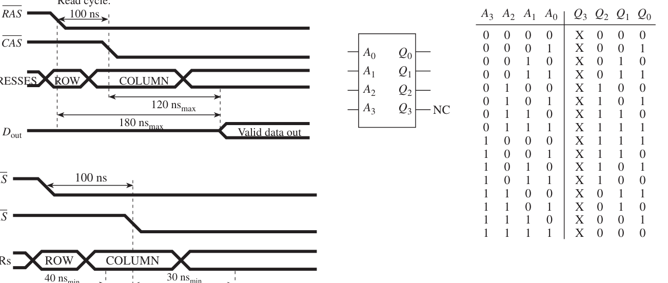
Din Valid data in
16–33. (a) Hard disk (b) DVD (LDA); (2) and (3) Pulse: read address
32k * 8 bytes at 2001, 2002 (4000H); (4) Pulse: read data at address 4000H
16–37. (a) 8k * 8 (b) SMN_SEL, MON_SEL
17–17. A high-level language (FORTRAN, BASIC,
(c) A000H–BFFFH (d) E000H–FFFFH
| E16–1. (a) The D flip-flop only captures data at | write and understand. Its disadvantage is |
|---|---|
| the instant C is pressed. | that the programs are not memory efficient. |
(b) Outputs are all stuck LOW. 17–19. (a) LOW (b) LOW
Chapter 17 (c) HIGH
(d) HIGH 17–1. A microprocessor-based system would be 17–21. U6a and U6b are drawn as inverted-input used whenever calculations are to be made, NAND gates to make the logical flow of decisions based on inputs are to be made, a the schematic easier to understand. memory of events is needed, or a modifi-
17–23. (a) IN instruction, RD is pulsed LOW.
(b) OUT instruction, WR is pulsed LOW.
17–25. (1) A8toA15 = FEH
lar location or device within the system.
(2) IO/M = HIGH
(3) WR is pulsed LOW/HIGH 74LS244
17–29. 2010 3E
| I0 | O0 | 2011 | 04 | ||
|---|---|---|---|---|---|
| I1 | O1 | 2012 | 3D | ||
| I2 | O2 | 2013 | CA | ||
| From | I3 | O3 | To | 2014 | 10 |
| Input | Data | 2015 I4 Switches | 20 O4 Bus | ||
| I5 | O5 CE from address decoder | 2016 2017 I6 2018 I7 | C3 12 O6 20 O7 | ||
| RD from | 17–31. OEa AD3 AD4 AD5 AD11 AD12 | LCD_SL OEb 0 0 0 1 1 | KEL_SL μp control bus 1 0 0 1 1 |
17–7. The input port has three-stated outputs so
| AD13 | 0 | 0 | |
|---|---|---|---|
| that it can be disabled when it is not being | AD14 | 0 | 0 |
| read. | AD15 | 0 | 0 |
17–9. 216(65,536)
E17–1. (a) LOW
17–11. It stores the contents of the accumulator (b) Press C
(c) Put 7C on the switches, make OE¿ = 0 (data appear on the data bus), press C 17–13. Instruction decoder and register: register
[data appear at output port if OE¿ (G) is LOW]. receives the machine language code and produces the internal control signals re-
quired to execute the instruction. Chapter 18
18–1. Because it has RAM, ROM, I/O Ports, and
a Timer/Counter on it 18–3. Extra 4 K ROM, 128 bytes RAM, 16 bit Timer/Counter, 1 interrupt
18–7. 80H-FFH ADD A,#05H
MOV P1,A 18–9. By reading the two bank-select bits
| (D0H.3, D0H.4) in the PSW | 18–21. | |||
|---|---|---|---|---|
| 18–11. (a) | A = 40H | (b) | A = 88H | |
| (c) | A = 88H | (d) | A = 40H | X8 |
A8
18–13. (a) MOV P3,#0C7H (b) MOV R7,P1 A12
(c) MOV A,#55H (d) MOV A,@R0
| (e) MOV P0,R1 | A9 |
|---|---|
| A13 | X4 |
18–15. START: MOV A,#20H
LOOP: MOV P1,A X2 P3.4
INC A A14 X3
| JMP START | A11 | |
|---|---|---|
| A = 75H | A = F5H | A15 |
| 18–17. (a) | (b) |
X4 (c) A = EBH
Appendix E VHDL Language Reference
Library-Entity-Architecture Model
Figure E–1 is a sample VHDL program showing the syntax rules and language format of a basic program.
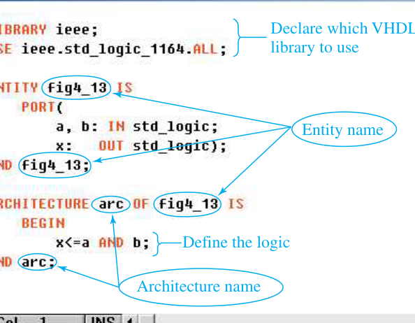
Figure E–1 VHDL program model showing the syntax for Library, Entity, and Architecture
Program, Entity, and Architecture Naming Conventions
Valid VHDL names can consist of letters, numbers, and the underscore (_) character [hyphens (-) are not allowed]. The name must start with a letter and cannot contain spaces.
Valid Names Invalid Names
| fig4_13 | fig4-13 | (cannot use hyphen) |
|---|---|---|
| boolean3 | boolean 3 | (cannot use space) |
| counter_5_a | counter_5.a | (cannot use period) |
Comments can be placed within a VHDL program to document a particular statement or group of statements. Any words preceded by a double hyphen (--) are considered to be a comment for documentation purposes and will be ignored by the VHDL compiler.
Sample Comments
-- Boolean solution to example 5-3 -- Problem C5-3 --
General VHDL Rules
VHDL logical operators have no order of precedence so the order must be explicitly
defined using parentheses. For example, the Boolean equation x = a + bc must be sult of the operation on the right-hand side to the left-hand side.) Also note that VHDL is not case-sensitive so the letters a, b, and c could have been capitalized, but the convention used by most VHDL programmers is to only capitalize the reserved keywords like AND, OR, PORT, ENTITY, and so on. (See Figure E–1.)
Logical Operators
The logic operators are used to perform Boolean bit-wise operations on individual bits or arrays of bits. (Example: x 6= a AND b;)
Operator Description
| AND | And |
|---|---|
| OR | Or |
| NAND | Not-And |
| NOR | Not-Or |
| XOR | Exclusive-Or |
| XNOR | Exclusive-Nor |
| NOT | Complement |
Relational Operators
The relational operators are used to test the relative values of two scalar types. The result is a Boolean true or false value. [Example: IF a * b THEN result *�"001". This is interpreted as “if the logic (a less than b) is true, then the bit string "001" is moved to the variable result.”]
Operator Description
| = | Equality |
|---|---|
| /= | Inequality |
| 6 | Less than |
| 6= | Less than or equal |
| 7 | Greater than |
| 7= | Greater than or equal |
The arithmetic operators are used to perform mathematical operations. (Example: sum_ string6=astring+bstring+cin;) The following is a partial list of the arithmetic operators.
Operator Description
| + | Addition |
|---|---|
| - | Subtraction |
| & | Concatenation |
| * | Multiplication |
> Division
| ** | Exponentiation |
|---|---|
| mod | Modulus |
| rem | Remainder |
| abs | Absolute value |
| sll | Shift left |
| srl | Shift right |
Data Types
The data type defines the type of value that can be used with the specified input, output, or internal signal. The most common data types used are as follows:
Type Values
| bit | '0', '1' |
|---|---|
| std_logic | '0', '1', 'U', 'X', 'Z', 'W', 'L', 'H', '-' |
| integer | Integer values |
| bit_vector | Multiple instances of '0', '1" |
| std_vector | Multiple instances of '0', '1', 'U', 'X', 'Z', 'W', 'L', 'H', '-' |
std_logic Data Type Values
The values that the std_logic data type can have are defined as follows:
Value Description
| '0' | Logic 0 |
|---|---|
| '1' | Logic 1 |
| 'U' | Uninitialized |
| 'X' | Unknown |
| 'Z' | High impedance |
| 'W' | Weak unknown |
| 'L' | Weak 0 |
| 'H' | Weak 1 |
| '-' | Don’t care |
fig5_62.vhd A vector with 3 elements Selected signal assignment for i = 3, 2, 1 then 0 ex6_10.vhd Loop 4 times
input (0) input (1) input (2) (c,d)
Figure 6–24
| output level sent to X | Figure 5–62 | ||||||||||
|---|---|---|---|---|---|---|---|---|---|---|---|
| Declare | SIGNAL | "input" | before | BEGIN | Make | assignments | after BEGIN | Note: Single | quotes for bits and | double quotes | for vectors |
Declare which VHDL Entity name
| library to use | Note: VHDL has no order |
|---|---|
| of precedence so | proper grouping. |
parentheses are required for Define the logic
Architecture name ex5_17.vhd
3-bit internal SIGNAL result
Assign vector elements compare_8b.vhd a2
| alb | aeb |
|---|---|
| agb | to outputs |
y0 y7 Sensitivity list
Figure 8–19
Figure 8–5
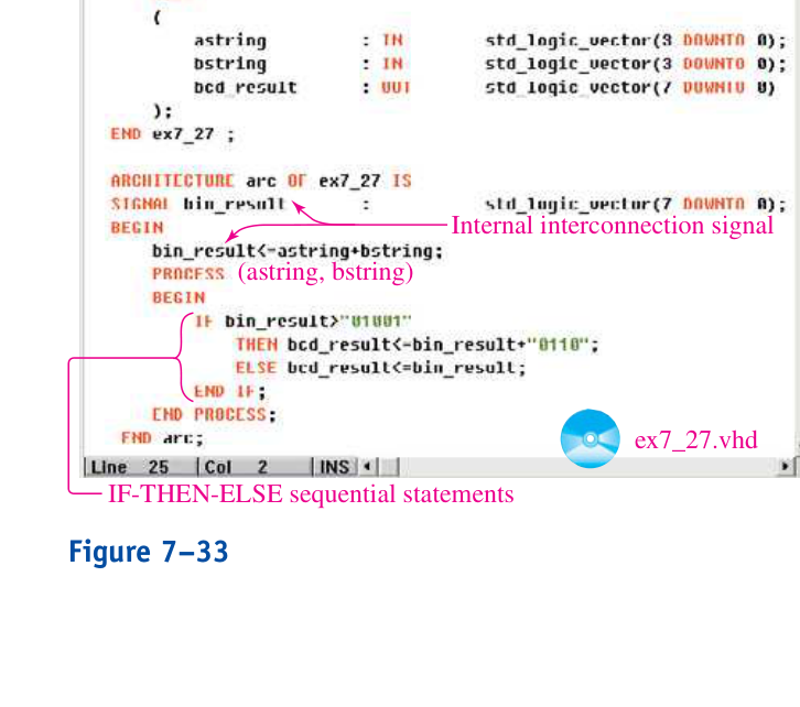
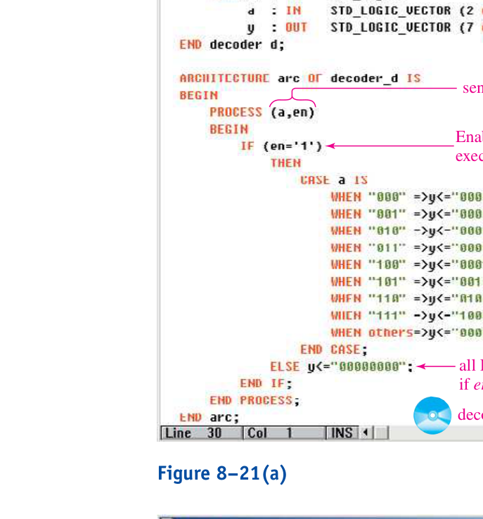
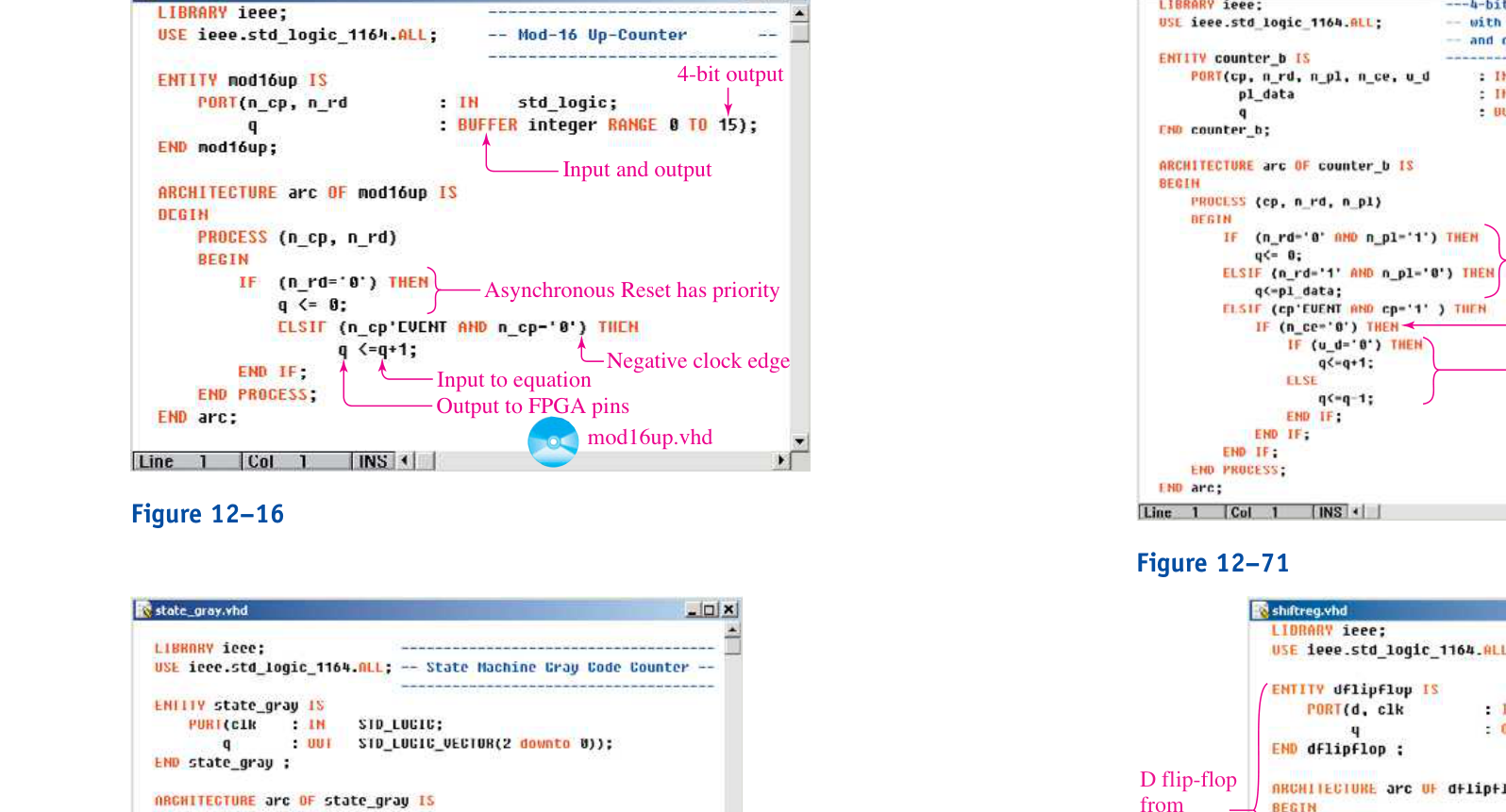
4-bit output Asynchronous Reset has priority Negative clock edge
Input and output mod16up.vhd Defines a new the allowable
Assign binary to q state_gray.vhd
to next state. based on value
Input to equation of state.
Appendix F Review of Basic Electricity Principles
Definitions for Figure F–1
through a pipe R
+ I –
Figure F–1 Series circuit used to illustrate Ohm’s law.
| voltage = volts | (V), for example, 12 V, 6 mV | |
|---|---|---|
| current = amperes | (A), for example, 2 A, 2.5 mA | |
| resistance = ohms(�), | for example, | 100�,4.7k� |
Common Engineering Prefixes
Prefix Abbreviation Value
| Mega- | M | 1,000,000 or 106 |
|---|---|---|
| kilo- | k | 1,000 or 103 |
| milli- | m | 0.001 or 10-3 |
| micro- | m | 0.000001 or 10-6 |
The current (I) in a complete circuit is proportional to the applied voltage (V) and inversely proportional to the resistance (R) of the circuit (see Figure F–2). Formulas I =V R V = I * R R =V I V
| I | R |
|---|---|
| Figure F–2 | Ohm’s law circle. |
EXAMPLE F–1
(a) Determine the current (I) in the circuit of Figure F–1 if V = 10V and
(b) Recalculate the current if R = 4�.
doubled to 4� in (b). R = 10�. (e) What voltage would be required in (d) if you only need one-half that current?
(f) If V = 12V in Figure F–1, what resistance is required to limit the cur(g) To limit the current to 1 A in (f), what resistance would you need?
Solution:
| I =V | R= 10V |
|---|---|
| (a) | 2�= 5A |
| I =V | R= 10V |
| (b) | 4�= 2.5A |
(c) As the resistance to current flow doubled, the current dropped to one-half.
| (d) | V = I * R = 2A * 10�= 20V |
|---|---|
| (e) | V = I * R = 1A * 10�= 10V |
Note we only need one-half the voltage to get one-half the current.
| R =V | I= 12V |
|---|---|
| (f) | 2A= 6� |
| R =V | I= 12V |
| (g) | 1A= 12� |
Note that, to reduce the current to 1 A, we needed to increase the circuit’s
resistance.
Apply the values listed below to the circuit of Figure F–1 to determine the unknown quantity.
| (a) I | = | 2 mA, | R | = | 4 k�, | V | = | __________? |
|---|---|---|---|---|---|---|---|---|
| (b) I | = | 6 mA, | R | = | 200 k�, | V | = | __________? |
| (c) I | = | 24 mA, | V | = | 12 V, | R | = | __________? |
| (d) I | = | 100 mA, | V | = | 5 V, | R | = | __________? |
| (e) V | = | 5 V, | R | = | 50 k�, | I | = | __________? |
| (f) V | = | 12 V, | R | = | 600 �, | I | = | __________? |
Solution:
| (a) | V = I * R = 2mA * 4k�= (2 * 10-3A) * (4 * 103�) = 8V | ||
|---|---|---|---|
| (b) | V = I * R = 6mA = 200k�= (6 * 10-6A) * (200 * 103�) = 1.2V | ||
| R =V | 12V | 12V | |
| (c) | I= | 24mA= | = 500k�(or0.5M�) |
24 * 10-6A
| R =V | 5V | |
|---|---|---|
| (d) | I= | 100mA= 50� |
| I =V | 5V | |
| (e) | R= | 50k�= 100mA |
| (f) I =V | 12V | |
| R= | 600�= 20mA |
EXAMPLE F–3
A series circuit has two or more resistors end to end. The total resistance is
equal to the sum of the individual resistances (RT = R1 + R2). Also, the
| age | (VS = VR1 + VR2). | |
|---|---|---|
| Find the current in the circuit (I), the voltage across R1 | (VR1), | and the |
| voltage across R2 | (VR2) | in Figure F–3. |
| R1 | 8 kΩ | VR1 |
I
| VS | 10 V | |
|---|---|---|
| R2 | 2 kΩ | VR2 |
| Figure F–3 | A series circuit used to derive the voltage divider equation. |
Solution:
RT = 8k�+ 2k�= 10k� 10V
I = 10k�= 1mA VR2 = 1mA * 2k�= 2V
Notice that the voltage across any resistor in the series circuit is proportional to the size of the resistor. That fact is used in developing the voltage- divider equation: R2 VR2 = VS * R1 + R2 2k� = 10V * 2k�+ 8k� = 2V
EXAMPLE F–4
Use the voltage-divider equation to find Vout in Figure F–4. (Vout is the voltage from the point labeled Vout to the ground symbol.)
| R1 | 4 kΩ |
|---|---|
| VS | 12 V |
Vout
| R2 | 2 kΩ | Vout |
|---|---|---|
| Figure F–4 | Circuit used to calculate the output voltage (Vout) with respect |
to ground. Solution: 2k� Vout = 12V * 2k�+ 4k� = 4V
EXAMPLE F–5
A short circuit occurs when an electrical conductor is purposely or inadvertently placed across a circuit component. The short causes the current to bypass the shorted component. Calculate Vout in Figure F–5. 4 kΩ Vout
12 V 2 kΩ Short Ground (V = 0)
| Figure F–5 | A short circuit across the | 2k� | resistor forces the output to zero V. |
|---|---|---|---|
| Solution: Vout is connected directly to ground; therefore, | Vout = 0V. of the 12-V supply is dropped across the | All 4@k� | resistor. |
EXAMPLE F–7
An open circuit is a break in a circuit. This can be done purposely by an electronic switching component, or it could be a circuit fault caused by a bad connector or burnt-out component. This break will cause the current to stop flowing to all components fed from that point. Calculate Vout in Figure F–7. Open 4 kΩ I =0A 12 V Vout 2 kΩ
| Figure F–7 | An open circuit causes current to stop flowing. |
|---|---|
| Solution: Because | I = 0A, |
V2k�= 0A * 2k�= 0V Vout = V2k�= 0V
Calculate Vout in Figure F–8.
I =0A 4 kΩ 12 V 2 kΩ Open
Figure F–8 An open circuit below the measurement point allows the entire
Solution: Because I = 0A,
Vdrop(4k�) = 0A * 4k�= 0V Vout = 12V - Vdrop = 12V
Note:
This is probably the hardest concept to understand. Another way to explain why the entire supply reaches Vout is to assume that an open circuit can be
| modeled by an extremely large resistance, let’s say, | 10M�. | If you then ap- |
|---|---|---|
| ply the voltage-divider equation to the circuit with | 10M� | in place of the |
open, the calculation will be 10,002,000
Vout = 12V * 10,002,000 + 4,000= 11.995V The symbol for a battery is seldom drawn in schematic diagrams. Figure F–9 is an alternative schematic for a series circuit. Solve for Vout. +12 V 4 kΩ Vout 2 kΩ
Figure F–9 Series circuit drawn without the battery symbol. 2k� Vout = 12V * 2k�+ 4k� = 4V
A relay’s contacts or a transistor’s collector–emitter can be used to create opens and shorts. Figure F–10(a) uses a relay to short one resistor in a series circuit (relay operation is described in Section 2–6). Sketch the waveform at Vout in Figure F–10(a). +12 V 4 kΩ Vout
| R1 | 2 kΩ | |
|---|---|---|
| Cp | 5 V | R1 |
0 V (a) 5 V Cp 0 V
| R1 | R1 |
|---|---|
| energized | de-energized |
4 V Vout 0 V (b)
Figure F–10 Using a relay to intermittently short the 2@k� resistor.
2@k� resistor and making Vout = 0V. When the coil is deenergized, the 2k� Vout = 12V * 2k�+ 4k� = 4V The clock oscillator (Cp) and Vout waveforms are given in Figure F–10(b).
Review Questions
F–1. What value of voltage will cause 6 mA to flow in Figure F–1 if
R = 2k� (3 V, 0.333 V, or 12 V)? _________ (increased/decreased). F–3. In a series voltage-divider circuit like Figure F–3, the larger resistor will have the larger voltage across it. True or false?
VR2 will be close to __________ (0 V/10 V). _________ (6 V/12 V). F–6. A short circuit causes current to stop flowing in the part of the circuit not being shorted. True or false? F–7. The current leaving the battery in Figure F–5 _________ (increases, decreases) if the short circuit is removed. F–8. The short circuit in Figure F–6 causes Vout to become 12 V because
| the current through the | 2@k� | resistor becomes 0 A. True or false? |
|---|---|---|
| F–9. In Figure F–7, the voltage across the | 2@k� | resistor is the same as that |
| across the | 4@k� | resistor. True or false? |
| F–10. If the | 4@k� | resistor in Figure F–8 is doubled, Vout will _________ |
(increase/decrease/remain the same)?
Answers to Review Questions
F–1. 12 V F–6. False
F–2. Decreased F–7. Decreases
F–3. True F–8. False
F–4. 0 V F–9. True
F–5. 6 V F–10. Remain the same
Problems
F–1. Refer to Figure F–1 to solve for the unknown quantities in the fol-
lowing table. [Example: For part (A), calculate the resistance if V = 12V
| Voltage | Current | Resistance |
|---|---|---|
| A | 12 V | 4 A |
| B | 8 V | 2 A |
| C | 100 V | 20� |
| D | 6 V | 2� |
| E | 6 A | 2� |
| F | 0.5 A | 5� |
F–2. Repeat problem 1 for the following table.
| Voltage | Current | Resistance |
|---|---|---|
| A | 12 mV | 3mA |
| B | 6 V | 2 mA |
| C | 100 mV | 20k� |
| D | 8 V | 2M� |
| E | 6 mA | 3k� |
| F | 0.5mA | 5k� |
lowing table.
| VS | R1 | R2 | Vout |
|---|---|---|---|
| A | 18 V | 6k� | 3k� |
| B | 18 V | 3k� | 6k� |
| C | 12 V | 20k� | 20k� |
| D | 6 V | 1k� | 100k� |
F–4. Refer to the original Figure F–4 to solve for Vout given the following open- and short-circuit conditions. Vout
| A | Short R1 |
|---|---|
| B | Short R2 |
| C | Open R1 |
| D | Open R2 |
Answers to Problems
F–1(a). 3� F–3(a). 6 V
F–1(b). 4� F–3(b). 12 V
F–1(c). 5 A F–3(c). 6 V
F–1(d). 3 A F–3(d). 5.94 V
F–1(e). 12 V
F–1(f). 2.5 V F–4(a). 12 V
F–4(b). 0 V
F–2(a). 4k� F–4(c). 0 V
3k� F–4(d). 12 V
F–2(b).
F–2(c). 5mA
F–2(d). 4mA
F–2(e). 18 V
F–2(f). 2.5 mV
Appendix G Schematic Diagrams for Chapter-End Problems
(This item omitted from WebBook edition)
(This item omitted from WebBook edition)
(This item omitted from WebBook edition)
(This item omitted from WebBook edition)
(This item omitted from WebBook edition)
(This item omitted from WebBook edition)
(This item omitted from WebBook edition)
(This item omitted from WebBook edition)
(This item omitted from WebBook edition)
Appendix H 8051 Instruction Set Summary*
*Courtesy of Intel Corporation.
Index
| 555 IC timers | ADC controllers | schematic symbol, 63 |
|---|---|---|
| astable operation, 698–704 | implementation, 605 | timing analysis, 68 |
| block diagram, 699 | process state diagram, 606 | truth tables, 63, 65 |
| monostable operation, 704–707 | simulation file for, 608 | AND-OR-INVERT gates, 201–205 |
| one-shot operation, 705 | state machine implementation, 607 | configurations, 203 |
| 8051 microcontroller, 816–847. See also | Adder circuits | defined, 202, 214 |
| Microcontrollers | basic, 276 | in SOP implementation, 204 |
| addressing modes, 825–826 | BCD, 290–292 | Answers, problem, 893–916 |
| ALE/PROG, 819 | block diagrams, 280–281 | AOIs. See AND-OR-INVERT gates |
| analog-to-digital converter interface, 835 | full-adder, 277–280 | Applications |
| applications, 831–835 | half-adder, 276–277 | 8051 microcontroller, 831–835 |
| architecture, 817–822 | VHDL, 285–287 | alarm encoder for microcontroller, 360–361 |
| arithmetic operations, 830–831 | Addition | analog multiplexer, 362–363 |
| assembly language, 826 | binary arithmetic, 261–262 | BCD adder circuit, 290–292 |
| block diagram, 818 | hexadecimal, 271–273 | controlled inverter, 245–247 |
| data acquisition and control system application, | two’s complement, 270 | counter circuits, 564–570 |
| 835–845 | Address bus, 796, 810 | data acquisition and control system, 835–845 |
| EA/VPP, 820 | Address decoders, 796 | data acquisition system (DAS), 738–741 |
| family, 817 | Address decoding, 778, 779, 788 | digital LCD thermometer, 782–783 |
| with input/output, 837 | Address spaces, 820–821 | FPGA, 147–150, 295–301 |
| instruction set, 825 | Addresses, 359, 369 | Karnaugh map, 211–213 |
| instruction set summary, 942–946 | Advanced Low-Power Schottky (ALS), 404 | microprocessor address decoding, 359–360 |
| instruction timing, 831 | Alphanumeric data, 18, 23 | multiplexed display, 363–364 |
| interfacing external memory to, | Altera CPLDs, 115 | numbering systems, 20–22 |
| 823–824 | Altera Cyclone II family, 420–421 | parallel binary comparator, 245 |
| keyboard interface, 834 | Altera LPM flip-flop, 467–469 | parity error-detection system, 244 |
| logical and bit operations, 827–829 | ALUs. See Arithmetic logic units | PROM look-up table, 781–782 |
| module, 836–838 | Analog comparators, 520–521 | sequential, 536 |
| pin configuration, 819 | Analog multiplexer switch, 740 | serial data multiplexing for microcontroller, |
| port 0, 818 | Analog multiplexer/demultiplexer, 357–358 | 361–362 |
| port 1, 818 | Analog representation, 717–718 | shift registers, 647–651 |
| port 2, 819 | Analog systems, 3, 23 | S-R flip-flop, 434 |
| port 3, 819 | Analog waveforms, 4, 5, 6 | synchronous counter ICs, 592–595 |
| program branch instructions, 826–827 | Analog-to-digital converters (ADCs), 5, 7, 604, | two’s-complement adder/subtractor circuit, |
| PSEN, 820 | 717 | 287–289 |
| RST, 819 | 8051 microcontroller interface, 835 | Application-specific integrated circuits (ASICs), |
| time delay, 831–835 | counter-ramp, 729–730 | 116, 121 |
| XTAL1, XTAL2, 820 | data acquisition system (DAS), 740–741 | defined, 150–151 |
| 8085A microprocessor, 798–808. See also | defined, 717, 747 | hard-coded logic function, 121 |
| Microprocessors | integrated-circuit, 733–738 | Architecture, 799, 810 |
| architecture, 799, 810 | interface module, 838 | Architecture body, 124, 150 |
| assembly language, 807 | interfacing linear temperature sensor to, 743 | Arithmetic |
| basic I/O, 803–805 | MultiSIM simulation, 737–738 | BCD, 274–275 |
| CPU, 800 | need for, 717 | binary, 261–266 |
| CPU functional block diagram, 799 | op amp, 718 | hexadecimal, 271–274 |
| design, 798 | parallel-encoded, 728–729 | two’s complement, 269–270 |
| features, 798–799 | specification definition, 727 | Arithmetic circuits, 275–281 |
| LDA instruction execution, 801 | successive-approximation, 730–733 | adder, 276 |
| machine language, 807–808 | AND gates, 63–65 | block diagrams, 280–281 |
| pin configuration, 799 | associative law of multiplication for, 162 | full-adder, 277–280 |
| STA instruction execution, 802 | Boolean equation, 64 | half-adder, 276–277 |
| AC waveforms, 485, 526 | commutative law of multiplication for, 162 | MSI, 275 |
| Accelerometers, 523 | defined, 63 | Arithmetic logic units (ALUs), 292–295, 798 |
| Accumulators | electrical analogy, 64 | defined, 292, 302, 798, 810 |
| defined, 798, 810 | enable/disable functions, 70–72 | function select, 292 |
| load, 801–802 | forming from two NAND gates, 196 | function table, 293 |
| store, 802–803 | in ICs, 73–74 | logic symbol, 293 |
| Active clock edge, 486, 526 | inverted-input, 178, 179 | mode control, 292 |
| Active-LOW, 189, 214, 442, 470 | MultiSIM analysis, 68–69 | Arithmetic operations, 830–831 |
Note: Page numbers in boldface type indicate end-of-chapter glossary definition for the term.
| ASICs. See Application-specific integrated circuits | commutative law of addition and multiplication, | BCD-to-seven-segment, 343 |
|---|---|---|
| (ASICs) | 162 | defined, 343, 369 |
| Assemblers, 805, 810, 847 | distributive law, 162 | Gray code, 345 |
| Assembly language | laws and rules, 162–166 | Column address strobes (CAS), 788 |
| defined, 798, 810 | laws and rules summary, 166 | Combinational logic, 157–162, 430 |
| mnemonics, 807 | ORed rules, 164–165 | circuit simplification, 167–172 |
| programs, writing, 805–808 | Boolean equations | defined, 157, 215, 470 |
| Associative law of addition and multiplication, | defined, 96 | encoder design with, 331 |
| 162 | drawing digital logic for, 132–133 | with multiplexers, 352–353 |
| Astable multivibrators, 685–687 | AND gate, 64 | Common-anode LED display, 570–571, 612 |
| 555, 698–704 | inverter, 80 | Common-cathode LEDs, 571 |
| defined, 681 | NAND gate, 81 | Commutative law of addition and multiplication, |
| MultiSIM simulation, 703 | NOR gate, 84 | 162 |
| operation, 685–686 | OR gate, 65 | Comparators, 313–316, 709 |
| Schmitt trigger, 685 | Boolean reductions | analog, 520–521 |
| Asynchronous, 435, 470 | defined, 157, 214 | binary, 313 |
| Asynchronous counters, 543, 612 | equation forms, 201 | defined, 245, 253, 313, 369 |
| ATM-thermal printer interface, 608–611 | VHDL proof, 158–162 | LPM, 365–366 |
| Automatic Reset, 502–503, 526 | Borrows, 262, 302 Bubble pushing, 188–189 | magnitude, 313–314, 370 symbols, 698 |
| BASIC language, 806, 807, 810 | Buffers, 401, 781 | VHDL, using IF-THEN-ELSE, 316–318 |
| BCD adders | defined, 422, 656, 667, 788 | Compilers, 122, 151, 805, 810 |
| correction, using IF-THEN-ELSE, 298–299 | octal IC, 781 | Complement, 80, 96, 432, 470 |
| defined, 290 | three-state, 656–657 | Complementing switch, 287 |
| IC, 291 | Burn in, 707, 709 | Complex programmable logic devices (CPLDs), |
| illustrated, 290 | Bus contention, 757, 788 | 116, 119 |
| MultiSIM simulation, 291–292 | Buses, 247, 363, 733 | Altera, 115 |
| BCD decoders, 318, 324 | address, 796, 810 | connecting multiple I/O to, 523–524 |
| BCD-to-binary conversion, 340–343 | control, 740, 796, 811 | defined, 119, 151 |
| BCD-to-seven-segment decoder, 572–573 | data, 32, 656, 667, 740, 796, 811 | internal structure of, 119 |
| Bias, 43, 56 | defined, 253, 369, 747 | nonvolatile characteristic, 119 |
| BiCMOS, 409, 422 | external, 796 | Components, 662, 667 |
| Bidirectional, 657, 667 | Bytes, 755, 788 data bus, 796, 810 | Concatenation, 329, 369, 455, 470 Concurrent assignments, 251 |
| I/O ports, 847 | CAD (computer-aided design), 151 | Concurrent statements, 278, 302 |
| outputs, 357, 369 | Capacitors | Conditional jump, 807 |
| Binary adder | charge/discharge rates, 681–685 | Conditional signal assignments, 296, 302 |
| block diagram, 281 | charging formula transposition, 682 | Continuous conversions, 730, 747 |
| MultiSIM simulation, 284–285 | in time durations, 681 | Control buses, 796, 811 |
| Binary arithmetic, 261–266 | voltage, 683, 685 | Controlled inverters, 245–247, 253 |
| addition, 261–262 | Carry-in, 261, 302 | circuit illustration, 246 |
| division, 265–266 | Carry-out, 261, 277, 302 | defined, 245 |
| multiplication, 264–265 | CAS (column address strobes), 788 | FPGA, 250 |
| subtraction, 262–264 | Cascade, 541 | MultiSIM simulation, 246–247 |
| Binary numbering system (base 2), 8–10 | CASE statements, 455 | Conversion |
| conversion to hexadecimal, 15–17 | CDs (compact discs), 786 | BCD-to-binary, 340–343 |
| defined, 23 | Cells (Karnaugh map) | continuous, 730 |
| hexadecimal conversion to, 15 | adjacent, 206–207, 214 | d, 343 |
| Binary strings, 245, 253 | defined, 205, 214 | data, 628 |
| Binary weighting factors, 8–10, 719, 747 | input variable correspondence, 205 | Gray code, 344–345 |
| Binary words, 281, 302 | number determination, 205 | parallel-to-serial, 629 |
| Binary-to-coded-decimal system (BCD), 17–18 | Celsius thermometer, 841–843 | serial-to-parallel, 631–633 |
| addition, 274–275 | Central processing units (CPUs), 798, | time, 730, 747 |
| arithmetic, 274–275 | 810 | Conversion time, 747 |
| conversion, 17–18 | Charge/discharge rates, 681–685 | Counter-ramp A/D converters, 729–730 |
| defined, 17 | Chip Planner, 174, 176, 214 | Counters |
| Binary-to-octal decoding, 319–320 | Chips, 50, 56 | asynchronous, 543, 612 |
| Bipolar transistors, 45–48, 405, 422 | Clock Enable, 650, 667 | divide-by-N, 548–559, 612 |
| Bistable multivibrators, 681 | Clock waveform | down-counter, 546–547 |
| Bit-addressable memory, 822, 847 | frequency, 30 | glitch-free, 558–559 |
| Bits (binary digits), 11, 23 | period, 30 | Gray code, 600–601 |
| Block Design File (bdf), 131–132 | periodic, 29–30 | Johnson shift, 633–635 |
| Block diagrams | timing, 29–31 | LPM, 599–600 |
| 555 IC timer, 699 | Clocks, 441, 470 | modulus of, 537 |
| 8051 microcontroller, 818 | Closed-loop feedback circuitry, 651, 667 | MSB, 567 |
| adder circuit, 280–281 | CMOS (complementary metal oxide | program, 800, 811 |
| arithmetic circuit, 280–281 | semiconductor) | ring shift, 633–635 |
| binary adder, 281 | advantages, 3 | ripple, 541–548, 613 |
| decoders, 327 | availability, 408–410 | synchronous, 543, 579–583, 613 |
| defined, 280, 302 | comparing logic families, 412–413 | up-counter, 547–548 |
| full-adder, 280 | defined, 53, 56, 406, 422 | up/down, 583–591, 613 |
| half-adder, 280 | devices, handling, 407 | VHDL, 595–598 |
| monostable multivibrator, 688 | gates, 95 | CPLDs. See Complex programmable logic devices |
| octal decoder, 327 | hex inverter, 53, 54 | CPUs (central processing units), 798, 810 |
| shift register, 627 | interfacing to TTL, 415–416 | Crystal, 707, 710 |
| two-gate, 688 | logic family, 405–410 | Crystal oscillators, 707–708 |
| Block editors, 122, 151 | multiplexers, 347 | Current |
| Boolean algebra, 162–172 | NAND gates, 407 | input/output, 388–391 |
| ANDed rules, 163–164 | NOR gates, 407 | sink, 389, 423 |
| associative law of addition and multiplication, 162 | TTL interfacing to, 414–415 | source, 389, 423 |
| device family data sheet, 881–887 | defined, 7, 23 | DVDs (Digital Versatile Disk), 787 |
|---|---|---|
| family, 420–421 | hexadecimal conversion to, 16 | Dynamic RAMs (DRAMs), 765–771 |
| propagation delay, 500–501 | number system conversion to, 8 Decimal-to-BCD encoders. See also Encoders | controllers, 768–770 data sheet, 767 |
| D flip-flops, 441–450. See also Flip-flops | function table, 332 | defined, 758, 765, 788 |
| with asynchronous Set and Reset, 448–450 | illustrated, 332 | delay lines, 769, 770 |
| creating with block design method, 446 | MultiSIM simulation, 334–335 | memory cell, 765–766 |
| for debouncing, 512, 513 | truth table, 331 | Read cycle timing, 768 |
| defined, 436 | Decimal-to-binary conversion, 10–12 | Refresh cycle timing, 768 |
| function table, 442 | Decoders, 800 | refresh period, 766 |
| gated, 436–437 | 1-of-8, 320 | sample, 770 |
| IC, 441–443 | 3-line-to-8-line, 320 | storage capacitor, 766 |
| from J-K flip flop, 462 | BCD, 318, 324 MultiSIM simulation, 443 | Write cycle timing, 768 block diagrams, 327 |
| octal, 465–466, 657 | defined, 318, 369 | ECL. See Emitter-coupled logic |
| simulation file for, 448, 450 | hexadecimal, 324–325 | Edge-triggered devices, 441, 470 |
| VHDL description, 445–448 | implemented in VHDL, 326–330 | Edge-triggered J-K flip-flops, 453–457 |
| D latches, 437–441 | instruction, 800, 811 | defined, 453 |
| IC, 437–439 | LPM, 366–367 | function table, 454 |
| simulation file for, 440 | octal, 321–324, 327–330 | negative edge, 453 |
| VHDL description, 439–440 | Decoding | VHDL description, 455–457 |
| VHDL design file, 440 | 3-bit binary-to-octal, 319–320 | Electrical noise, 238, 253 |
| Data acquisition and control system application, | defined, 318 | Electrically erasable PROM (EEPROM), 772, 774, |
| 835–845 | microprocessor address, 359–360 | 777, 788 |
| 8051 microcontroller module, 836–838 | Decoupling | Electricity |
| ADC interface module, 838 | defined, 403, 422 | engineering prefixes, 924 |
| applications, 841–845 | power supply, 403, 515 | Ohm’s law and, 925–930 |
| celsius thermometer, 841–842 | Delay lines, 769, 770, 788 | open circuits, 928 |
| DAC interface module, 838–841 | Delay-gate ICs, 490 | principles, 924–932 |
| hardware, 836–841 | Demultiplexers, 354–358. See also Multiplexers | series circuits, 926 |
| integrating solar radiometer, 843–845 | analog, 357–358 | units, 924 |
| temperature-dependent PWM speed control, | configurations, 355 | voltage-divider equation, 927 |
| 843 | connections, 357 | Electromagnetic interference (EMI), 403, 422 |
| Data acquisition system (DAS), 738–741 | as data distributor, 354 | Electrostatic discharge (ESD), 407 |
| analog multiplexer switch, 740 | defined, 354, 369 | Emitter-coupled logic (ECL), 410–412, 422 |
| analog-to-digital converter, 740–741 | functional diagram, 355 | comparing logic families, 412–413 |
| defined, 738, 747 | logic symbol and diagram, 356 | interfacing, 418 |
| illustrated, 739 | waveform simulation editor, 355 | logic family, 410–412 |
| programmable-gain instrumentation amplifier, | Dependency notation, 888 | OR/NOR gate, 410–411 |
| 740 | Differential amplifiers, 410, 422 | series, 410 |
| sample-and-hold circuit, 740 | Differential measurements, 736, 747 | supply voltage, 410 |
| Data bits, 626, 667 | Differential nonlinearity, 727 | Enable function |
| Data buses, 656, 733, 796 | Digital representation, 3–6, 717–718 | defined, 70, 97 |
| bidirectional, 796 | Digital sequencers, 633, 667 | MultiSIM simulation, 72 |
| defined, 32, 667, 811 | Digital signals, 29–31 | AND/OR gates, 70–72 |
| Data conversion, 628, 667 | clock waveform timing, 29–31 | Enabled, 434, 451, 470 |
| Data loggers, 6, 7 | illustrated, 29 | Encoders |
| Data selectors. See Multiplexers | timing diagram, 29 | decimal-to-BCD, 331 |
| Data sheets, 491–494, 852–887 | Digital states, 451, 470 | defined, 331, 369 |
| 74ABT244 octal buffer/line driver (3-state), | Digital systems, 3, 23 | design with combinational logic, 331 |
| 867–870 | Digital waveforms, 4, 6 | for microcontroller, 360–361 |
| 74HC00 quad two-input NAND gate, 854–862 | Digital-to-analog converters (DACs), 5, 717 | octal-to-binary, 335–337 |
| 74LV00 quad 2-input NAND gate, 863–866 | binary-weighted, 719–720 | priority, 335, 370, 729 |
| 7400 quad two-input NAND gate, 393–395 | defined, 717 | VHDL octal priority, 338–339 |
| 7476/74LS76 dual J-K flip-flop, 491–494 | integrated-circuit, 723–726 | Encoding, 331–339 |
| Cyclone II device family, 881–887 | interface module, 838–841 | Energized relay coils, 39, 56 |
| KA741 single operational amplifier, 871–874 | MultiSIM simulation, 725 | Engineering prefixes, 924 |
| LM555 single timer, 875–880 | op amp, 718 | Entity declaration, 124, 151 |
| Web site links to, 852–853 | R/2R ladder, 720–722 | Enumeration types, 600, 612 |
| Data transfer rate, 786 | specification definition, 727 | Equivalent circuits |
| Data transmission, 655, 667 | Diodes, 37 | defined, 162, 215 |
| Data types, VHDL, 919 | defined, 42–43, 56 | distributive law for, 163 |
| De Morgan’s theorem, 177–191 | forward-biased, 43, 44 | NAND gates for, 197 |
| active-LOW, 189, 214 | reverse-biased, 43 | TTL NAND, 386–388 |
| bubble pushing, 188–189, 214 | as switches, 42–45 | Erasable-programmable read-only memory |
| defined, 177, 215 | voltage, 43 | (EPROMs), 771 |
| inversion bubbles, 177, 215 | DIP (dual-in-line package), 50, 56 | address decoding, 778, 779 |
| NAND gate application, 177 | Disable function | data sheet, 775 |
| NOR gate application, 178 | defined, 70, 97 | defined, 788 |
| product-of-sums (POS) and, 202 | MultiSIM simulation, 72 | electrically erasable (EEPROM), 772, 774, 777, |
| sum-of-products (SOP) form, 183 | AND/OR gates, 70–72 | 788 |
| for three/more variables, 177 | Disabled, 451, 470 | Flash memory, 772, 774, 777 |
| Debouncing. See also Switches | Discharge transistors, 699 | Program cycle, 776 |
| cross-NAND method, 511 | Distributive law, 162 | programming, 775–777 |
| D flip-flop method, 512, 513 | Divide-by-N, 612 | Read cycle, 776 |
| methods, 510 | Division, binary arithmetic, 265–266 | representative, 777 |
| Schmitt method, 511 | Don’t care, 187, 215, 322, 369 | simplified diagram and memory cell, 774 |
| Decimal numbering system (base 10), 7–8 | Double quotes, 192 | UV, 772–773 |
| BCD conversion to, 17–18 | Down-counters, 546–547 | Error indicator, 241, 253 |
| conversion to hexadecimal, 16 | Dual-in-line package (DIP), 50 | ESD (electrostatic discharge), 407 |
| Exclusive-OR gates, 237 | Fusible-link PROMs, 772, 788 | CMOS, 53–54 |
|---|---|---|
| defined, 237, 253 | configuration as DIPs, 51 | |
| operation, 238 | Gated S-R flip-flops, 435–436 | A/D converter, 733–738 |
| parity generator/checker, 242 | Gates, 62–97 | D/A converter, 723–726 |
| Exponential charge/discharge, 682, 710 | AND, 63–65 | delay-gate, 490 |
| External Access, 820, 847 | defined, 63, 97 | full-adder, 281–285 |
| External buses, 796 | enable/disable functions, 70–72 | AND gates in, 73–74 |
| External memory, interfacing to, 823–824 | exclusive-NOR, 238–239 | monostable multivibrator, 690–695 |
| External resistors, 691 | exclusive-OR, 237 IC, using, 73–74, 92–94 | octal, 465, 471 OR gates in, 73–74 |
| Fall time, 397, 422 | inverter, 79–80 | parity generator/checker, 242–244 |
| Fan-out, 388–391, 422 | multitap delay, 496 | ripple counter, 559–563 |
| Fast-look-ahead carry, 283, 303 | NAND, 80–83 | shift register, 638–646 |
| Faults, 74–79, 97 | NOR, 83–85 | stepper motor driver, 654–655 |
| Ferromagnetic material, 651, 667 | NOT, 80 | synchronous counter, 588–590 |
| Field-programmable gate arrays (FPGAs), 116, | OR, 65 | troubleshooting techniques, 74–79 |
| 119–121. See also Programmable logic | AND-OR-INVERT, 201–205, 214 | volatile, 789 |
| devices (PLDs) | SSI, 352 | Integrating slope converters, 730 |
| applications, 147 | strobe, 434 | Integrating solar radiometer, 843–845 |
| applications with VHDL and LPMs, 295–301 | summary, 94–96 | Interfacing, 740, 747 |
| connecting multiple I/O to, 523–524 | timing analysis, 67–70 | Interfacing logic families, 413–420 |
| controlled inverter, 250–252 | troubleshooting, 74–79 | Internal resistors, 691 |
| defined, 119, 151 | in TTL and CMOS families, 95 | Interrupts, 800, 811 |
| design applications with LPMs, 365–368 | universal, 196–201, 215 | Inversion bar, 80, 97 |
| design applications with VHDL, 247–252 | unused, 403 | Inversion bubbles, 177, 215 |
| design flow, 122 | waveform generation, 86 | Inverters |
| electrical characteristics, 420–421 | Glitches, 369, 549, 612 | Boolean equation, 80 |
| illustrated, 120–121 | Gray code, 343–344, 369 | controlled, 245–247, 253 |
| look-up table (LUT), 119 | counter, 600–601 | defined, 49, 56 |
| parallel binary comparator, 249–250 | defined, 343 | forming from NAND gates, 196 |
| programming, 141, 143–144 | four-bit, 344 | forming from NOR gates, 198 |
| Flash memory, 772, 774 | wheel, 344 | hex, 53, 56, 92 |
| Flip-flop memory circuitry, 117 | Groups, 247, 253 Flip-flops | as NOT gate, 80 Schmitt trigger, 503–509 |
| ac waveforms, 485 | Half-adder, 276–277, 280, 303 | symbol, 79 |
| active clock edge, 486 | Hall-effect switch, 521–522 | timing analysis, 80 |
| automatic Reset, 502–503 | Hand assembly, 805, 811 | truth table, 79 |
| D, 441–450 | Handshaking, 740, 747 D latch, 437–441 | I/O-mapped I/O, 803, 811 Handshaking signals, 650, 667 |
| defined, 471 | Hard disks, 784–786 | Jitter, 503, 526 |
| gated D, 436–437 | Hardware, 339, 370, 804 | J-K flip-flops, 450–465 |
| gated S-R, 435–436 | data acquisition and control system application, | automatic power-up Reset, 502–503 |
| hold time, 486 | 836–841 | connected as toggle flip-flop, 463 |
| J-K, 450–465 | defined, 811 | D flip-flop from, 462 |
| metastable state, 490 | requirements for I/O programming, 803–805 | defined, 450 |
| octal, 657 | Hertz (Hz), 30 | edge-triggered, 453–457 |
| propagation delay, 487 | Hex, 92, 97 | in flip-flop formation, 462 |
| race condition, 485 | Hex inverters, 53, 56, 92 | IC, 457–465 |
| setup time, 485 | Hexadecimal arithmetic, 271–274 | master-slave, 450–453 |
| S-R, 431–435 | addition, 271–273 | MultiSIM simulation, 459 |
| T, 463–464 | subtraction, 273 | synchronous operating modes, 450 |
| time parameters, 485–502 | Hexadecimal decoders, 324–325 | toggles, 450 |
| Float, 75, 97, 513, 526, 644, 667 | Hexadecimal numbering system (base 16), | Johnson shift counter, 86–92 |
| Floating-gate MOSFET, 773–774, 788 | 14–17 | defined, 86, 97 |
| Floorplan Editor Display, 215 | conversions, 15–17 | MultiSIM simulation, 87–88 |
| Floppy disks, 784–786 | defined, 14, 23 | use of, 87 |
| Flowcharts, 806, 811 | PC I/O devices, 22 | waveform generation illustration, 86 |
| Flux lines, 651, 667 | High-impedance state, 644, 667 For Loop, 247, 253 | Johnson shift counters, 633–634, 635 High-order bits, 283, 303 |
| Forward-biased diodes, 43, 44 | Hold time, 486, 526 | Karnaugh maps (K-maps), 183, 205–211 |
| Four-bit full-adder ICs, 281–285 | Hysteresis, 503, 526 FPGAs. See Field-programmable gate arrays | adjacent cells, 206–207, 214 cell correspondence, 205 |
| Frequency, 30, 31, 56 | IEEE/IEC logic symbols, 94–96, 888–892 | cell number determination, 205 |
| Full-adder, 277–281. See also Arithmetic | IF-THEN-ELSE statements, 298–299, 303 | cells, 205, 214 |
| circuits | octal decoder VHDL program with, 330 | defined, 205, 215 |
| block diagram, 280 | VHDL comparator using, 316–318 | encircling adjacent cells in, 207 |
| carry-out, 277 | IN FFH, 804–805 | illustrated, 206–207 |
| defined, 277, 303 | Input ports, 797 | reduction procedure, 206 |
| four-bit ICs, 281–285 | Input/output | truth tables, 206 |
| logic diagram, 278 | 8051 microcontroller with, 837 MultiSIM simulation, 279–280 | wraparound, 209 I/O-mapped, 803, 811 |
| sum function, 277 | memory-mapped, 803, 811 | LAB (Logic Array Block), 215 |
| Function select, 292, 303 | multiple, connecting to CPLD or FPGA, | Latches |
| Function tables, 242, 243, 253, 431 | 523–524 | D, 437–441 |
| ALU, 293 | practical considerations, 514–524 | defined, 430, 471 |
| D flip-flop, 442 | Instantiations, 662, 667 | octal, 657 |
| decimal-to-BCD encoder, 332 | Instruction decoders, 800, 811 | transparent, 430–431, 472, 657, 668 |
| defined, 471 | Instruction registers, 798, 811 | LCDs (liquid-crystal displays), 572, 612, 782, 788 |
| edge-triggered J-K flip-flop, 454 | Instruction timing, 831–835 | Least significant bit (LSB), 11, 12, 23, 276 |
| octal-to-binary encoder, 335 | Integers, 285, 303 | LEDs. See Light-emitting diodes |
| defined, 417, 423 | expansion, 762–765, 780–781 | 555 astable multivibrator, 703 |
|---|---|---|
| illustrated, 417 | external, 823–824 | ADC, 737–738 |
| optocoupler for, 517–518 | Flash, 772, 774, 777 | BCD adder, 291–292 |
| Level-triggered master-slave J-K flip-flops, 452 | locations, 755 | binary adder, 284–285 |
| Library declaration, 124, 151 | magnetic, 754, 784–786, 789 | controlled inverter, 246–247 |
| Library of Parameterized Modules (LPM) | mapping, 780 | D flip-flops, 443 |
| adder/subtractor, 299–301 | nonvolatile, 151 | DAC, 725 |
| comparator, 365–366 | optical, 754, 786–787, 789 | decimal-to-BCD encoder, 334–335 |
| counter, 599–600 | read-only, 771–778 | electro-mechanical relay switching, 41–42 |
| decoder, 366–367 | read/write, 758 | full-adder, 279–280 |
| defined, 295, 303 | semiconductor, 754–777 | AND gate, 68–69 |
| flip-flop, 467–468 | Memory-mapped I/O, 803, 811 | J-K flip-flop, 459 |
| flip-flop with asynchronous control, 468–469 | MEMS (Micro-Electro-Mechanical Systems), | Johnson shift counter, 87–88 |
| FPGA applications with, 295–301, 365–368 | 522–523 | MOD-5 counter, 550–551 |
| multiplexer, 367–368 | Metastable state, 490, 526 | monostable multivibrator, 693 |
| shift register, 660–662 | Microcontrollers. See also 8051 microcontroller | multiplexer, 350–351 |
| Light-emitting diodes (LEDs) | alarm encoder for, 360–361 | octal decoder, 323–324 |
| common-anode, 570–571, 612 | defined, 360, 370, 808, 817, 847 | parallel transmission, 36 |
| common-cathode, 571 | octal D flip-flops for, 465–466 | ripple counter, 545–546 |
| display decoders, 570–583 | serial data multiplexing for, 361–362 | Schmitt triggers, 505–506 |
| driving, 516–517 | Microprocessor-based systems, 795 | serial transmission, 35–36 |
| Linear IC temperature sensors, 742–743 | example illustration, 796 | seven-segment LED display, 573–574 |
| Liquid-crystal displays (LCDs), 572, 612, 782, | software control of, 798 | shift registers, 630–631, 643 |
| 788 | Microprocessors, 794–812. See also 8085A | simplification of logic circuits, 171–172, |
| Load accumulators, 801–802 | microprocessor | 190–191 |
| Logic Array Block (LAB), 215 | address decoding, 359–360 | switching circuits, 51 |
| Logic cells, 215 | defined, 370, 740, 747, 795, 811 | T flip-flop, 463–464 |
| Logic families, 384–423 | instruction execution within, 800–803 | TTL NAND, 386–387 |
| Altera Cyclone II, 420–421 | internal architecture of, 798 | two’s complement adder/subtractor circuit, |
| CMOS, 405–410 | I/O software comparison, 798 | 288–289 |
| comparing, 412–413 | manufacturers, 808–809 | MultiSIM Logic Converter, 171–172, 190 |
| comparing structure objects, 412–413 | support circuitry, 795 | Multitap delay gates, 496 |
| ECL, 410–412 | survey of, 808–809 | Multivibrators, 681–698 |
| interfacing, 413–420 | Mnemonics, 798, 807, 811 | astable, 681, 685–687, 701 |
| performance specifications, 412 | MOD-5 counters, 549–551 | bistable, 681 |
| TTL, 385–405 | block diagram, 549 | defined, 681, 710 |
| types of, 384 | MultiSIM simulation, 550–551 Logic gates. See Gates | monostable, 681, 687–698 state diagram, 550 |
| Logic probes, 75, 97 | waveform, 549 | NAND gates, 80–83 |
| Logic pulsers, 75, 97 | MOD-8 counters, 548 | Boolean equation, 81 |
| Logic state, 34, 56 | MOD-10 counters, 556–557 | CMOS, 407 |
| Logic symbols, 94–96, 888–892 | MOD-16 counters, 544–546, 547–548 | De Morgan’s theorem application, 177 |
| Logical operators, 918 | Mode control, 292, 303, 640, 667 | defined, 80 |
| Look-up tables (LUTs) | Modulus, 537, 612 | equivalent logic circuit using, 197 |
| defined, 119, 151, 788 | Monitor programs, 797, 811 | forming AND gates from, 196 |
| illustrated, 120–121 | Monostable multivibrators, 687–698 | forming inverters from, 196 |
| PROM, 781–782 | 555, 704–707 | forming NOR gates from, 198 |
| Low-order inputs, 283, 303 | block diagram, 688 | forming OR gates from, 197 |
| Low-Power Schottky, 404 | defined, 681 | logic circuit implementation with, 196 |
| LPM. See Library of Parameterized Modules | integrated circuit, 690–695 | symbols, 80, 81 |
| LSB (least significant bit), 11, 12, 23 | MultiSIM simulation, 693 retriggerable, 690, 695–698 | timing analysis, 82 truth tables, 81, 82 |
| Machine code, 801, 811 | MOSFETs (metal oxide semiconductor field-effect | TTL form, 80 |
| Machine language, 805–808 | transistors) | universal capability, 196–201 |
| Macro-functions, 247, 253, 661 | defined, 405, 423 | Negative edge, 453, 471 |
| Magnetic memory, 784–786 | driving relay and AC motor, 520 | Netlist Viewer, 175, 176, 184, 215 |
| data transfer rate, 786 | floating-gate, 773–774, 788 | Next state, 601, 612 |
| defined, 754, 789 | N-channel, 405, 406 | NMOS, 405, 406, 423 |
| floppy disk, 784–786 | as ON/OFF switches, 406 | Node Finder, 137, 138 |
| hard disk, 784–786 | P-channel, 406 | Noise, 452, 471 |
| MRAM, 786 | switching characteristics, 406 | Noise margin, 391–396, 423 |
| Magnetoresistive random access memory | Most significant bit (MSB), 11, 12, 24, 567 | Nonlinearity, 727, 747 |
| (MRAM), 786, 788 | MRAM (magnetoresistive random access memory), | Nonmonotonic, 727, 747 |
| Magnitude comparators, 313–314, 370 | 786, 788 | Nonvolatile memory, 119, 151 |
| Mask ROMs, 771, 789 | MSB (most significant bit), 11, 12, 24, 567 | NOR gates, 83–85 |
| Master-slave J-K flip-flops, 450–453. See also | Multiplexed display application, 363–364 | CMOS, 407 |
| J-K flip-flops | Multiplexers, 346–354 | De Morgan’s theorem, 178 |
| defined, 451, 471 | analog, 357–358, 362–363 | defined, 83 |
| level-triggered, 452 | CMOS, 347 | forming from NAND gates, 198 |
| pulse-triggered, 451, 452 | combinational logic functions with, 352–353 | forming inverters from, 198 |
| MCS-51 instruction set, 943–946 | data select input codes, 346 | repetitive waveform, 86 |
| Medium-scale-integration (MSI) circuits, 260, | defined, 346, 370 | symbol, 83 |
| 275, 303 | eight-line, 348–350 | truth table, 84 |
| Memory, 786–787, 797. See also Random-access | four-line, 353–354 | TTL form, 83 |
| memory (RAM) | functional diagram, 346 | universal capability, 196–201 |
| addresses, 755, 789 | logic diagram, 347 | NOT, 81, 97 |
| banks, 359 | LPM, 367–368 | NOT gates. See Inverters |
| bit-addressable, 822, 847 | for microcontroller, 361–362 | Numbering systems |
| cells, 758, 765–766, 774, 789 | MultiSIM simulation, 350–351 | applications of, 20–22 |
| concepts, 755–758 | TTL form, 347 | BCD, 17–18 |
| comparison of, 18 | defined, 32, 57 | effect on ripple counter, 543 |
|---|---|---|
| decimal (base 10), 7–8 | MultiSIM simulation, 36 | Pull-down resistors, 514, 526–527 |
| hexadecimal (base 16), 14–17 | PC printer port use, 33 | Pull-up resistors, 401, 423, 513–514, 527 |
| octal (base 8), 12–14 | Parallel-encoded A/D converters, 728–729 Parallel-to-serial conversion, 629 | Pulse stretching, 680, 710 Pulse-triggered master-slave J-K flip-flops, 451, |
| Octal D flip-flops, 465–466 | Parentheses, 180 Octal decoders, 321–324 | 452, 471 Parity, 238, 253 |
| block diagrams, 327 | Parity error-detection system, 244 | Quad, 92, 97 |
| defined, 321 | Parity generator/checker, 241–244 | Quartus II software, 126–147 |
| with enable input, 329 | construction of, 242 | arithmetic operators, 174 |
| implementation with vectors, 328 | eight-bit, 243 | Block Design Editor, 127 |
| logic symbol and diagram, 321 | error indicator, 241 | block design file creation, 131–132 |
| MultiSIM simulation, 323–324 | even, 241, 242 | Chip Planner, 174, 176, 214 |
| pin configuration, 321 | from exclusive-OR gates, 242 | circuit connections, 134 |
| VHDL program with Boolean equations, | five-bit, 243 | Compilation Report, 174 |
| 327–328 | IC, 242–244 | computer screen displays, 123 |
| VHDL program with IF-THEN-ELSE, 330 | with input bus configuration, 247–248 | defined, 126–127 |
| Octal ICs, 465, 471, 657, 667 | odd, 241, 242 | digital logic for Boolean equation, 132–133 |
| Octal numbering system (base 8), 12–14 | Period, 30, 31, 57 | enter symbol mode, 247 |
| conversions, 12–14 | Periodic clock waveform, 29–30 | Floorplan Editor Display, 215 |
| defined, 12, 24 | Phototransistors | FPGA applications, 147–150 |
| uses, 12 | defined, 517, 526, 613 | FPGA programming, 141, 143–144 |
| Octal priority encoder, 338–339 | as input to latching alarm system, 517 | functional simulation, 140–141 |
| Octal-to-binary encoders, 335–337 | resistance, 581 | inputs and outputs, 137–138 |
| Ohm’s law, 925–930 | PLA (programmable logic array), 116–117 | logic testing, 144 |
| Ones catching, 452, 471 | PLDs. See Programmable logic devices | main screen, 127 |
| One’s complement, 267, 303 | PMOS, 405, 406, 423 | Netlist Viewer, 175, 176, 184, 215 |
| Op amps, 718, 747 | Pole pairs, 651, 668 | New Project Wizard, 128–131 |
| Opcodes, 807, 811 | Polling, 740 | Node Finder, 137, 138 |
| Open circuits, 928 | PORT MAP keyword, 662, 664, 668 | pin assignment, 141–142 |
| Open-drain (OD) outputs, 401 | Port numbers, 804, 811 | project compilation, 134–135 |
| Open-collector (OC) outputs, 400–401, 423 | Positive edge, 441, 471 | project creation, 127–131 |
| Operands, 807, 811 | Positive feedback, 503, 526 | project re-compilation, 142–143 |
| Operating systems, 797, 811 | Power dissipation, 400, 423 | running, 123–126 |
| Optical interrupter switch, 518–520 | Power supply decoupling, 403, 515 | in simplified equations determination, 172–177 |
| Optical memory, 754, 786–787 | Power-up, 502, 526 | Text Editor, 127 |
| CD-Rs, 787 | Present state, 601, 613 | timing waveforms creation, 138–139 |
| CD-RWs, 787 | Priority encoders, 335, 370, 729 | tutorials, 126–147 |
| CDs, 786 | Problems | vector waveform file creation, 135–137 |
| defined, 789 | odd-numbered answers, 893–916 | VHDL design entry, 144–147 |
| DVDs, 787 | schematic diagrams, 933–942 Optocouplers | Quotes, 192 Process statement, 247, 253 |
| defined, 517, 526 | Product terms, 151 | R/2R ladder digital-to-analog converters (DACs) |
| for level shifting, 517–518 | Product-of-sums (POS) | analog output versus digital input, 722 |
| OR gates | De Morgan’s theorem and, 202 | current division, 721 |
| associative law of addition for, 162 | defined, 201–205, 215 | defined, 720 |
| Boolean equation, 65 | logic circuit, 203 | illustrated, 721 |
| commutative law of addition for, 162 | Products, 263, 303 | Race condition, 485, 527 |
| defined, 65 | Program counters, 800, 811 | Radix, 247, 253 |
| electrical analogy, 66 | Program instructions, 795–796 | Random-access memory (RAM), 758 |
| enable/disable functions, 70–72 | Program Store Enable, 820–821, 847 | defined, 789 |
| forming from three NAND gates, 197 | Programmable array logic (PAL), 116–118, 151 | dynamic, 765–771 |
| in ICs, 73–74 | Programmable logic array (PLA), 116–117, 151 | magnetoresistive (MRAM), 786 |
| inversion bubbles, 177 | Programmable logic devices (PLDs) | as read/write memory (RWM), 758 |
| with inverted inputs, 177 | application-specific integrated circuits (ASICs), | static, 758–765 |
| inverted-input, 178 | 116, 121 | use of, 758 |
| programmable, 116 | architecture, 116–121 | RAS (row address strobe), 789 |
| schematic symbols, 65, 66 | complex (CPLDs), 116, 119 | RC circuits, 502, 527 |
| truth tables, 65, 67 | defined, 112, 151 | Read-only memories (ROMs), 771–778. See also |
| Oscillation, 583, 612 | design flow, 113–115 | Memory |
| Oscillators | development boards, 115 | defined, 771, 789 |
| crystal, 707–708 | field-programmable gate arrays (FPGAs), 116, | erasable-programmable, 771 |
| defined, 707, 710 | 119–121 | mask, 771 |
| voltage-controlled, 707 | power of, 114 | programmable, 772 |
| Oscilloscopes, 29 | price of, 115 | Read/write memory (RWM), 758 |
| defined, 56 | sample illustration, 113 | Recirculating registers, 629–630, 641, 668 |
| illustrated, 29 | schematic capture, 113, 151 | Rectifier circuits, 515, 527 |
| pulse rise/fall times, 397 | simple (SPLDs), 116–117 | Redundancy, 211, 215 |
| OUT FEH, 805 | for solving logic designs, 122–126 | Reference voltage, 734, 747 |
| Output Enable, 656–657, 668 | types of, 116 | Refresh period, 766 |
| Output ports, 797 | Programmable read-only memories (PROMs), 772 | Register arrays, 800 |
| Oxide isolation, 405 | defined, 789 erasable, 771, 772–777 | Register banks, 821, 847 Registers, 465, 471. See also Shift registers |
| PAL (programmable array logic), 116–118 | fusible-link, 772 | commonly used, 655 |
| Parallel binary comparators, 245 | look-up tables (LUTs), 781–782 | defined, 655, 668 |
| FPGA, 249–250 | Programmable-gain amplifiers, 740, 747 | instruction, 798, 811 |
| illustrated, 245 | PROMs. See Programmable read-only memories | Relational operators, 918 |
| Parallel Enable, 645, 668 | Propagation delay, 397, 423 | Relays. See also Switches |
| Parallel format, 628 | for asynchronous input, 489 | defined, 38, 57 |
| Parallel Load, 588–590, 613, 627–628 | for clock to output, 489 | in digital circuits, 40 |
| energized relay coils, 56 | simulation, 578 | gated, 435–436 |
|---|---|---|
| MultiSIM simulation, 41–42 | three-digit display, 574, 575 | as storage register, 434 |
| normally closed (NC), 38 | VHDL description of, 577–578 | symbols, 432 |
| normally open (NO), 39 | SFRs (Special Function Registers), 821, 847 | synchronous, 435 |
| symbolic representation, 39 | Shaft encoder disks, 519 | timing analysis, 432–433 |
| timing diagram, 40 | Shift counters | SRAM (static random-access memory), 120 |
| Remainders, 262, 303 | defined, 633, 668 | Stack pointers, 800, 811 |
| Repetitive waveforms, 86, 97 | Johnson, 633–634, 635 | State diagrams, 543 |
| Representation, 32–37 | ring, 633–635 | ADC controller process, 606 |
| parallel, 32–36 | Shift registers, 626–668 | ATM-thermal printer interface, 609 |
| serial, 32 | basics, 627–629 | defined, 543, 613 |
| Reset | block diagram, 627 | MOD-5 counter, 550 |
| automatic, 502–503, 526 | defined, 626, 629, 668 | ripple counters, 543 |
| defined, 431, 471 | ICs, 638–646 | State machines |
| synchronous counters, 594 | LPM, 660–662 | ADC controller, 607 |
| Resolution, 718, 747 | MultiSIM simulation, 630–631, 643 | defined, 600, 613 |
| Retriggerable monostable multivibrators, 690, | parallel-load shift-right, 637 | for Gray code sequencer, 600–601 |
| 695–698 | parallel-to-serial conversion, 629 | implementation in VHDL, 600–611 |
| defined, 690, 695, 710 | recirculating, 629–630, 641, 668 | for multiple control inputs, 604–611 |
| nonretriggerable comparison, 695 | serial-in parallel-out, 638–639 | for stepper motor, 601–604 |
| output pulse width, 696 | serial-in shift-right, 636 | Statement labels, 807, 812 |
| timing chart, 696 | serial-to-parallel conversion, 631–633 | Static RAMs (SRAMs), 758–765. See also |
| Reverse-biased diodes, 43 | system design applications, 647–651 | Random-access memory (RAM) |
| Rewritable CDs (CD-RWs), 787 | three-state outputs, 643–644 | data sheet, 759 |
| Ring shift counters, 633–635 | universal, 640 | defined, 758, 789 |
| Ripple, 515, 527 | VHDL description of, 635–637 | functional diagram, 760 |
| Ripple blanking, 572, 613 | Sign bits, 267, 303 | logic symbols, 764 |
| Ripple carry, 283, 303 | Signal conditioning, 745 | memory expansion, 762–765 |
| Ripple counters, 541–548 | Signals | MOS technology, 758 |
| defined, 541, 613 | defined, 191, 215 | read operation, 761–762 |
| down-counter, 546–547 | digital, 29–31 | sample, 764 |
| ICs, 559–563 | handshaking, 650, 667 | timing waveforms, 761 |
| MOD-16, 544–546 | selected assignment, 192 | write operation, 762 |
| MultiSIM simulation, 545–546 | vector, 191–195 | Stator coils, 651, 668 |
| propagation delay effect on, 543 | Signed numbers, 296, 303 | Stepper motors |
| state diagram, 542 | Simple programmable logic devices (SPLDs), | defined, 651, 668 |
| up-counter, 547–548 | 116–117 | drive circuitry, 653 |
| waveforms, 542 | defined, 116, 151 | driver ICs, 654–655 |
| Rise time, 397, 423 | flip-flop memory circuitry, 117 | driving with shift registers, 651–655 |
| Rotors, 651, 668 | PAL architecture, 116, 117 | illustrated, 652, 653 |
| Row address strobe (RAS), 789 | PLA architecture, 116, 117 Simplification of logic circuits | pin configuration, 654 state machine for, 601–604 |
| Sample-and-hold circuits, 740, 747 | with Boolean Algebra, 167–172 | wiring, 655 |
| Saturation, 49, 57 | defined, 167 | Stepping angles, 651, 668 |
| Scalars, 353, 370 | MultiSIM examples, 171–172, 190–191 | Storage registers, 466, 471 |
| Schematic capture, 113, 151 | Simplified equations | Store accumulators, 802–803 |
| Schematic diagrams, problems, 933–942 | with Netlist Viewer technique, 184 | Strain gages |
| Schmitt triggers, 503–509 | Quartus II to determine, 172–177 | defined, 744 |
| astable multivibrator, 685 | Single quotes, 192 | foil type, 744 |
| for debouncing, 511 | Single-pole, double throw (SPDT) switches, 511, | in measuring force, 744 |
| defined, 503, 527 | 527 | signal conditioning for, 745 |
| inverting, 509 | Single-pole, single throw (SPST) switches, 509, | Strobe gates, 434, 471 |
| MultiSIM simulation, 505–506 | 527 | Strobes, 632, 668 |
| positive feedback, 503 | Sink current, 389, 423 | Structural approach, 662, 668 |
| switching characteristics, 504 | Skewed, 543, 613 | Substrate, 405, 423 |
| transfer function, 504, 505 | Small Computer Systems Interface (SCSI), 32 | Subtraction |
| Schottky TTL, 404 | Small-scale integration (SSI) logic gates, 352 | binary arithmetic, 262–264 |
| SCSI (Small Computer Systems Interface), 32 | SMDs (surface-mount devices), 54, 55, 57 | hexadecimal, 273 |
| Seconds (s), 30 | Software, 339, 798 | two’s complement, 270 |
| Selected Signal Assignment, 192, 215 | celsius thermometer, 842 | Successive division, 11, 16 |
| Semiconductor memory, 754–778, 789 | defined, 370, 811 | Successive-approximation A/D conversion, |
| Sequential applications, 536 | integrating solar radiometer, 845 | 730–733 |
| Sequential circuits | temperature-dependent PWM speed control, | defined, 730, 747 |
| analysis of, 538–541 | 844 | timing waveforms, 732 |
| defined, 613 | Solar radiation data-logger system, 6 | voltage-level contributions, 732 |
| Sequential logic, 117, 430, 471 | Solder bridge, 75, 76 | Summation symbol (sigma), 261 |
| Sequential operations, 251, 253 | SOP. See Sum-of-products | Sum-of-products (SOP), 116, 152 |
| Sequential statements, 298–299, 303 | Source current, 389, 423 | AOI IC implementation, 204 |
| Serial format, 628 | SPDT (single-pole, double throw) switches, 511, | form, 183, 201, 215 |
| Serial representation, 32 | 527 | logic circuit, 203 |
| of binary numbers, 32 | Special Function Registers (SFRs), 821, 847 | AND-OR-INVERT gates for implementing, |
| defined, 32, 57 | SPLDs. See Simple programmable logic devices | 201–205 |
| MultiSIM simulation, 35–36 | SPST (single-pole, single-throw) switches, 509, | truth tables from, 202 |
| Serial-to-parallel conversion, 631–633 | 527 | use of, 202 |
| Series circuits, 926 | S-R flip-flops, 431–435 | variables, 202 |
| Set, 431, 471 | application, 434 | Sums, 261, 303 |
| Setup time, 443, 471, 485, 527 | asynchronous, 435 | Superimpose, 362, 370 |
| Seven-segment decoders, 570–583 | cross-NAND, 432 | Support chips, 795 |
| BCD-to, 572 | cross-NOR, 431 | Support circuitry, 795, 812 |
| defined, 613 | defined, 431 | Surface-mount devices (SMDs), 54, 55, 57 |
| bounce, 509, 527 | defined, 49, 57, 423 | entering truth tables with, 191–195 |
|---|---|---|
| as clock input to toggle flip-flop, 510 | fan-out, 388–391 | selected assignment, 192 |
| complementing, 287 | gates, 95 | Vector Waveform File (vwf), 135–137 |
| debouncing, 509–513 | improved series, 403–405 | VHDL (VHSIC Hardware Description Language) |
| diode, 42–45 | input/output current, 388–391 | 4-line multiplexer, 353–354 |
| in electronic circuits, 37 | input/output voltage, 391–396 | adders with integer arithmetic, 285–287 |
| Hall-effect, 521–522 | integrated circuit, 50 | architecture body, 124, 150 |
| manual, 37 | interfacing to CMOS, 414–415 | arithmetic operators, 918 |
| ON/OFF resistances, 37 | inverter circuit schematic, 51 | circuit reduction proof, 158–162 |
| optical interrupter, 518–520 | logic family, 385–405 | comments, 192 |
| relay, 38–42 | multiplexers, 347 | comparator, using IF-THEN-ELSE, |
| SPDT, 511, 527 | NAND, 386–388 | 316–318 |
| SPST, 509, 527 | noise margin, 391–396 | components and instantiations, 662–666 |
| transistor, 45–48 | open-collector (OC) outputs, 400–401 | D flip-flop description, 445–448 |
| transistor-transistor logic (TTL), 49–51 | power dissipation, 400 | D latch description, 439–440 |
| Switching circuits, MultiSIM simulation, 51–52 | power supply decoupling, 403 | data types, 919 |
| Synchronous, 435, 471 | pulse-time parameters, 397–399 | decoder implementation in, 326–330 |
| Synchronous counters, 579–583 | Schottky, 404 | defined, 113, 152 |
| applications, 592–595 | totem-pole arrangement, 50, 57 | design entry, 144–147 |
| circuit connections, 580 | unused inputs/gates, 403 | edge-triggered J-K flip-flop description, |
| with component instantiations, 665 | voltage and current ratings, 388–397 | 455–457 |
| defined, 543, 613 | wired-output operation, 401–402 | entity declaration, 124 |
| high-speed multistage, 591 | Transition arrows, 605, 613 | by example, 920–923 |
| ICs, 588–590 | Transitions | FPGA applications with, 247–252, 295–301 |
| output waveforms, 580 | defined, 441, 472 | full-adder description, 278–279 |
| system design application, 581–583 | unconditional, 605, 613 | general rules, 918 |
| up/down, 583–591 | Transmission, 238, 253 | glitch-free counter description, 558–559 |
| Synthesizing, 122, 152 | Transparent latches, 430–431, 472, 657, 668 | language reference, 917–923 |
| System design applications. See Applications | Triggers | library declaration, 124 |
| Systematic approach, 205 | defined, 441, 472 Schmitt, 503–509 | logical operators, 918 For Loop, 247, 253 |
| T flip-flops | Troubleshooting techniques, 74–79, 97 | MOD-10 up-counter description, 556–557 |
| J-K flip-flop connected as, 463 | Truth tables | MOD-16 up-counter description, 547–548 |
| MultiSIM simulation, 463–464 | BCD-to-seven-segment decoder, 577 | naming conventions, 917 |
| Temperature-dependent PWM speed control, 843 | binary addition, 261 | octal priority encoder, 338–339 |
| Terminal Count, 584, 588, 613 | binary subtraction, 263 | Process statement, 247, 253 |
| Thermistors, 741–742, 747 | decimal-to-BCD encoders, 331 | program comments, 918 |
| with ADC, 742 | defined, 97 | program listing, 145 |
| characteristic curve, 741 | ECL OR/NOR, 411 | program model, 917 |
| defined, 717 | entering in VHDL with vector signal, | programs, reading, 124 |
| Three-state buffers, 656–657 | 191–195 | relational operators, 918 |
| Three-state outputs, 643–644, 668 | exclusive-NOR gate, 238 | seven-segment decoder description, |
| Thresholds, 505, 527 | exclusive-OR gate, 237 | 577–578 |
| Time constant, 701, 710 | AND gate, 63, 65 | shift registers description, 635–637 |
| Time delay, 831–835 | inverter, 79 | state machine implementation in, |
| Timing analysis | Karnaugh maps (K-maps), 206 | 600–611 |
| AND gate, 80 | NAND gate, 81, 82 | std_logic data type values, 919 |
| gates, 67–70 | NOR gate, 84 | text editor, 114, 122, 152 |
| inverter, 80 | OR gate, 65, 67 | truth tables with vector signal, 191–195 |
| NAND gate, 82 | from SOP expression, 202 | up-counter, 595–596 |
| S-R flip-flop, 432–433 | SOP form in building, 183 | up-down counter, 597–598 |
| Timing diagrams | TTL. See Transistor-transistor logic | Virtual ground, 718, 747 |
| defined, 29, 57, 67 | Two’s complement | Volatile ICs, 789 |
| relay, 40 | adder/subtractor circuit, 287–289 | Voltage regulators, 515, 527 |
| Timing waveforms, 496 | addition, 270 | Voltage-controlled oscillators (VCOs), |
| Toggles, 450–453, 471 | arithmetic, 269–270 | 707, 710 |
| Totem-pole arrangement, 50, 57 | to decimal number, 268–269 | Voltage-divider equation, 927 |
| Totem-pole output, 403, 423 | decimal number to, 267–268 | Voltages |
| Transceivers, 657–659 | defined, 263, 267, 303 | capacitor, 683, 685 |
| as bidirectional, 657 | negative numbers, 287 | input/output, 391–396 |
| defined, 657, 668 | numbers, 267 | reference, 734, 747 |
| octal, 659 | representation, 267–269 pin configuration, 659 | supply, 410 subtraction, 270 |
| Transducers, 718, 741, 747 | Type declaration, 192, 215 Transfer functions | Waveform generators, 86, 97 Waveform simulation editor, 124 |
| defined, 504, 527 | Unconditional transitions, 605, 613 | Waveform simulators, 123, 152 |
| Schmitt trigger, 504, 505 | Universal gates, 196–201, 215 | Web sites, 850–851 |
| Transistors, 37, 45–48 | Unsigned numbers, 298, 304 | Weighting factors |
| bipolar, 45–48, 405, 422 | Up-counters | for BCD bit positions, 340 |
| defined, 45, 57 | MOD-16, 547–548 | defined, 340, 370 |
| discharge, 699 | VHDL, 595–596 | powers-of-2 binary, 8 |
| NPN, 46 | Up/down-counters, 583–591 | WHEN-ELSE conditional signal statements, 296, |
| regions, 45 | defined, 583, 613 | 304 |
| as switches, 45–48 | function table, 584 | Wired-AND logic, 401–402, 423 |
| Transistor-transistor logic (TTL), 49–51, 405. See | VHDL, 597–598 also Switches | Wraparound, 209, 215 USB (Universal Serial Bus), 6 |
| bipolar transistors, 405 | User-recordable CDs (CD-Rs), 787 | Zener breakdown, 516, 527 |
| chip operation, 385 | UV-erasable PROM, 772–773 | Zero flags, 807, 812 |
Supplementary Index of ICs
This is an index of the integrated circuits (ICs) used in this book. Page numbers indicate where the IC is first discussed. Page numbers in boldface type indicate pages containing a data sheet for the device.
| 1N749 | Zener diode, 516 | 74148 | 8-input priority encoder, 335–337 |
|---|---|---|---|
| 2118 | Dynamic RAM, 768 | 74150 | 16-input multiplexer, 352 |
| 2147H | Static MOS RAM, 758–764 | 74151 | 8-input multiplexer, 348–352 |
| 2716 | 2K X 8 EPROM, 773 | 74154 | 1-of-16 decoder, 324–326 |
| 2732 | 4K X 8 EPROM, 778 | 74160 | Synchronous counter, 590 |
| 27C64 | EPROM, 853 | 74161 | Synchronous counter, 590 |
| 3242 | DRAM controller, 768 | 74162 | Synchronous counter, 590 |
| 4001 | Quad 2-input NAND gate, 92 | 74163 | Synchronous counter, 590 |
| 4008 | 4-bit full adder, 287 | 74164 | 8-bit shift register, 638–639 |
| 4011 | Quad 2-input NAND gate, 94 | 74165 | 8-bit shift register, 639–640 |
| 4049 | CMOS hex inverter, 53 | 74181 | 4-bit ALU, 292 |
| 4050 | Buffer, 415 | 74184 | BCD-to-binary converter, 341–343 |
| 4050B | Level-shifting buffer, 417 | 74185 | Binary-to-BCD converter, 341–342 |
| 40504B | CMOS level shifter, 417 | 74190 | BCD up/down counter, 588–589 |
| 4051 | Multiplexer/demultiplexer, 357 | 74191 | 4-bit binary up/down counter, 588–589 |
| 4052 | Multiplexer/demultiplexer, 357 | 74192 | BCD up/down converter, 567 |
| 4053 | Multiplexer/demultiplexer, 357 | 74193 | 4-bit binary up/down converter, 583 |
| 4077 | CMOS quad Ex-NOR gate, 238 | 74194 | 4-bit universal shift register, 640–643 |
| 555 | Timer, 698–703, 875–880 | 74244 | Octal 3-state buffer, 409 |
| 6800 | Motorola microprocessor, 795 | 74280 | Parity generator/checker, 242–244 |
| 6809 | Microprocessor, 359 | 74280b | Parity generator/checker, 747–748 |
| 68HC11 | Microcontroller, 465–466 | 74283 | 4-bit full adder, 295 |
| 7400 | Quad 2-input NAND gate, 55, 393–395 | 74395A | 4-bit shift (right) register, 644 |
| 7402 | Quad 2-input NOR gate, 83 | 74ABT244 | Octal buffer, 409, 867–870 |
| 7404 | Hex inverter, 50 | 74AHC16244 | Widebus octal buffer, 410 |
| 7405 | Buffer/driver, 401 | 74ALS112 | Negative edge-triggered flip-flop, 540 |
| 7406 | Inverter buffer/driver, 401 | 74ALS32 | OR gate, 419 |
| 7407 | Buffer/driver, 401 | 74F00 | NAND, 852 |
| 7408 | Quad 2-input AND gate, 73 | 74F112 | Flip-flop, 852 |
| 7411 | Triple 3-input AND gate, 73 | 74H106 | J-K flip-flop, 487 |
| 7414 | Schmitt trigger inverter, 503–506 | 74H71 | Master-slave flip-flop, 451 |
| 7421 | Dual 4-input AND gate, 73 | 74HC00 | High-speed CMOS NAND, 408, 852, 854–862 |
| 7427 | Triple 3-input NOR gate, 95 | 74HC192 | CMOS counter, 583 |
| 7430 | 8-input NAND gate, 107 | 74HC193 | CMOS counter, 583 |
| 7432 | Quad 2-input OR gate, 73 | 74HC1G00 | Single-gate NAND, 410 |
| 7442 | BCD-to-decimal decoder, 324 | 74HC280 | Parity generator/checker, 242–244 |
| 7447 | BCD-to-seven-segment converter, 343 | 74HC283 | 4-bit full adder, 283 |
| 7472 | Master-slave flip-flop, 451 | 74HC4543 | BCD-to-seven segment LCD decoder, 782 |
| 7473 | Master-slave flip-flop, 451 | 74HC86 | CMOS quad Ex-OR gate, 255 |
| 7474 | Dual D flip-flop, 441–445 | 74HCT00 | High-speed CMOS NAND, TTL compatible, 408 |
| 7475 | Quad bistable latch, 437–439 | 74HCT04 | Inverter, 419 |
| 7476 | Dual J-K flip-flop, 457, 491–494 | 74HCT08 | Quad 2-input AND gate, 520 |
| 7483 | 4-bit full adder, 281 | 74HCT138 | Octal decoder, 359 |
| 7485 | 4-bit magnitude comparator, 314 | 74HCT151 | Multiplexer, 362 |
| 7486 | Quad Ex-OR gate, 238 | 74HCT238 | Multiplexer/demultiplexer, 362 |
| 7490 | 4-bit decade counter, 559 | 74HCT273 | 8-bit D flip-flop, 465 |
| 7492 | Divide-by-12 counter, 559 | 74HCT4051 | Multiplexer/demultiplexer, 357 |
| 7493 | 4-bit binary ripple counter, 559 | 74HCT583 | 4-bit BCD adder, 291 |
| 74104 | Master-slave flip-flop, 451 | 74LS00 | NAND gate, 400 |
| 74105 | Master-slave flip-flop, 451 | 74LS01 | Open-collector NAND gate, 400 |
| 74109 | Dual J-K flip-flop, 461 | 74LS08 | AND gate, 419 |
| 74112 | Dual J-K flip-flop, 517 | 74LS112 | Dual J-K flip-flop, 458 |
| 74121 | Monostable multivibrator, 690 | 74LS138 | Address decoder, 778 |
| 74123 | Retriggerable monostable multivibrator, 690 | 74LS194 | Shift register, 643 |
| 74132 | Quad 2-input Schmitt NAND, 507 | 74LS244 | Buffer, 520 |
| 74138 | Octal decoder, 321 | 74LS245 | Octal three-state transceiver, 659 |
| 74139 | Dual 1-of-4 decoder/multiplexer, 355–356 | 74LS373 | Octal flip-flop, 441 |
| 74147 | 10-line-to-4-line priority encoder, 331–335 | 74LS374 | Octal flip-flop, 441 |
| 74LV00 | Low-voltage NAND, 863–866 | HM62W8512B | Static RAM, 765 |
|---|---|---|---|
| 74LVC8T245 | 8-bit transceiver, 660 | HM6264B | Static RAM, 765 |
| 74S124 | VCO, 698–703 | HM5165805 | Dynamic RAM, 770 |
| 74S154 | 1-of-16 decoder, 757 | IRF130 | Power MOSFET, 520 |
| 7805 | 5-V voltage regulator, 515 | KA741 | Operational amplifier, 871–874 |
| 8031 | Microcontroller, 817 | LF198 | Sample-and-hold circuit, 740 |
| 8051 | Microcontroller, 816–847, 853 | LH0084 | Programmable-gain instrumentation amplifier, 740 |
| 8052 | Microcontroller, 821 | LM35 | Linear temperature sensor, 520 |
| 8085 | Intel microprocessor, 795 | LM185 | Precision reference diode, 743 |
| 8085A | Microprocessor, 359 | LM339 | Analog comparator, 520 |
| 8155 | RAM with I/O, 824 | LM555 | Timer, 698–703, 875–880 |
| 8751 | Microcontroller, 817 | LM741 | Operational amplifier, 853 |
| 10124 | ECL level translator, 418 | MAX | 7000S CPLD, 119 |
| 10125 | ECL level translator, 418 | MC1408 | DAC, 723–724 |
| ADC0801 | Analog-to-digital converter, 834, 853 | MJ2955 | PNP power transistor, 653 |
| ADC0804 | Analog-to-digital converter, 734–737 | NE5034 | Analog-to-digital converter, 733–734 |
| AM3705 | Analog multiplexer circuit, 740 | PAL16L8 | SPLD, 117–118 |
| DAC0808 | Digital-to-analog converter, 723, 853 | UCN5804B | Stepper motor driver, 654–655 |
| EP2C35 | FPGA, 500–501, 881–887 | Z80 | Zilog microprocessor, 795 |
| 1 | 14 | VCC | 1 | 14 | VCC | 1 | 14 | VCC | 1 | 14 | VCC | 1 | 14 | VCC | ||||||
|---|---|---|---|---|---|---|---|---|---|---|---|---|---|---|---|---|---|---|---|---|
| 2 | 13 | 2 | 13 | 2 | 13 3 4 5 6 | 2 12 11 10 9 | 13 3 4 5 6 | 2 12 11 10 9 | 13 3 4 5 6 | 12 11 10 9 | 3 4 5 6 | 12 11 10 9 | 3 4 5 6 | 12 11 10 9 | ||||||
| GND | 7 | 8 | GND | 7 | 8 | GND | 7 | 8 | GND | 7 7414 | 8 7421 0 | GND 7427 1 | 7 7432 16 | 8 7442 VCC | ||||||
| 1 | 14 | VCC | 1 2 3 4 5 6 | 14 13 12 11 10 9 | VCC 2 3 4 5 6 | 1 13 12 11 10 9 | 14 2 3 4 5 6 | VCC 13 12 11 10 9 | 1 2 3 4 5 6 | 14 13 12 11 10 9 | VCC 2 3 4 5 6 | 1 3 4 5 6 7 | 2 14 13 12 11 10 | 15 A1 A2 A3 9 8 | A0 | |||||
| GND | 7 | 8 A2 | GND A1 f BI/RBO | 7 1 1 LT a | 8 16 14 3 3 | GND VCC VCC 14 12 | 7 Q0 RD1 D1 Cp1 | 8 1 1 3 3 | GND 16 14 2 g 14 12 4 | 7 7447 Q0 VCC 15 2 Q1 D2 13 | 8 7454 CP1 D0 2 13 RD1 E2-3 4 | GND 7474 1 Q1 15 D1 3 E0-1 13 | 8 7475 16 SD1 2 2 14 J1 4 | 9 7476 K1 Q1 15 13RD2 Q1 GND 13 | 7 | |||||
| RBI | 5 | 12 | b | 4 | 11 | SD1 | 4 | 11 Cp2 | VCC | 5 | 12 | GND | VCC | 5 | 12 | K2 | ||||
| A3 | 6 | 11 | c | 5 | 10 | Q1 | 5 | 10 | SD2 | D2 | 6 | 11 | Q2 | CP2 | 6 | 11 | Q2 | |||
| A0 | 7 | 10 | d | 6 | 9 | Q1 | 6 | 9 | Q2 | D3 | 7 | 10 | Q2 | SD2 | 7 | 10 | Q2 | |||
| GND | 8 | 9 | e | GND | 7 | 8 | GND A4 | 7 1 | 8 16 | Q2 7483 B4 | Q3 7485 B3 | 8 7486 1 | 9 7490 16 | Q3 7492 VCC | RD2 | 8 | 9 | J2 | ||
| ∑3 | ∑4 B3 | IA< B A3 CIN | A3 IA= B IA> B | 1 B2 A2 | 14 2 3 | VCC 13 12 | CP1 MR1 MR2 | 1 2 3 | 14 13 12 | CP0 NC 3 Q0 | CP1 2 NC 14 NC 4 | 1 15 2 COUT 3 13 | 14 2 13 3 12 4 | CP0 15 NC 14 Q0 13 | ||||||
| VCC | 5 | 12 | GND | A > B | 5 | 12 | A1 | 4 | 11 | NC | 4 | 11 | Q3 | NC | 4 | 11 | Q1 | |||
| ∑2 | 6 | 11 | B1 | A = B | 6 | 11 | B1 | 5 | 10 | VCC | 5 | 10 | GND | VCC | 5 | 10 | GND | |||
| B2 | 7 | 10 | A1 | A < B | 7 | 10 | A0 | 6 | 9 | MS1 | 6 | 9 | Q1 | MR1 | 6 | 9 | Q2 | |||
| A2 | 8 CP1 | 9 1 MR2 | ∑1 CP1 14 3 | GND 1 CP0 RD1 12 | 8 16 SD1 3 Q0 | 9 K1 Q1 14 J1 | B0 RD1 J1 Q1 GND | GND 1 RD2 MR1 K1 CP1 | 7 16 K1 2 2 3 K2 4 | 8 7493 VCC RD1 15 13 14 SD1 13 | MS2 74106 CP1 Q 2 NC J2 CP2 4 | 7 74109 1 1 15 RD2 J1 A1 13 | 8 74112 16 14 2 2 3 3 4 | Q2 74121 VCC VCC 15 13 14 12 13 | MR2 | 7 | 8 | Q3 | ||
| NC | 4 | 11 | Q3 | VCC | 5 | 12 | K2 | SD1 | 5 | 12 | CP2 | Q1 | 5 | 12 | K2 | A2 | 4 | 11 | Rext/Cext | |
| VCC | 5 | 10 | GND | CP2 | 6 | 11 | Q2 | Q1 | 6 | 11 | RD2 | Q1 | 6 | 11 | J2 | B | 5 | 10 | C | |
| NC | 6 | 9 | Q1 | SD2 | 7 | 10 | Q2 | Q1 | 7 | 10 | Q2 | Q2 | 7 | 10 | SD2 | Q | 6 | Q Q | 9 | Rint |
| A1 | 1 | 16 | VCC | A0 | 1 | 16 | VCC | Ea | 1 | 16 | VCC | I4 | 1 | 16 | VCC | ||||
|---|---|---|---|---|---|---|---|---|---|---|---|---|---|---|---|---|---|---|---|
| 1 | 14 | VCC | A1 | Eb B1 | I5 2 | 15 | Rext/Cext 1 | 2 | 15 | 0 | A0a | 2 | 15 | 2 2 | 15 13 | ||||
| RD1 | 3 I4 | 14 1 | Cext 1 16 | A2 VCC | 3 GND D6 | 14 Q1 Q2 Rext/Cext2 A2 D8 | 1 Q1 Q2 Cext2 6 B2 GND I3 | A1a 3 4 4 5 5 11 6 7 7 8 D7 1 | 3 12 13 11 12 10 RD2 9 10 8 9 1 16 | 14 E1 4 E2 5 E3 6 7 7 GND 8 24 VCC | A0b 2 13 3 12 4 11 5 10 6 9 74148 VCC A0 2 | I6 0a 4 1a 5 2a 6 3a 7 GND 8 74150 0 SR 23 | 3 A1b 13 0b 12 1b 11 2b 10 3b 9 74151 1 1 1 | 14 I7 4 I8 5 A2 6 A1 7 GND 8 74154 24 16 2 | A3 I3 13 I2 12 I1 11 I9 10 A0 9 74163 VCC VCC 23 | ||||
| I5 | 2 | 15 I6 | EO GS I7 | D5 D4 4 | 3 4 13 | 22 21 I3 | D9 D10 D2 | I2 I1 D3 I0 | 2 I5 5 4 6 | 15 3 3 20 13 19 | I4 4 14 D11 I6 D12 | 2 21 3 4 D1 5 | 3 A2 14 5 4 6 | 22 D0 3 20 13 19 | A1 Q0 14 A3 Q1 E1 | CP | 2 | 15 | TC |
| EI | 5 | 12 A2 | I2 I1 | D1 D0 A1 | 7 8 7 | 18 17 10 | D13 D14 I0 | Y Y E E Y | 5 S0 9 7 10 | 12 7 6 16 10 15 | I7 8 11 D15 S1 S0 | 6 17 6 8 CEP 9 | 7 15 11 9 7 10 | 18 D3 6 16 10 15 | E0 Q3 11 14 CET 13 | D2 | 5 | 12 | Q2 |
| GND | 8 | 9 | A0 | S3 | 11 | 14 | S1 | GND GND | 8 12 | 9 13 | S2 S2 74164 | 10 GND 74165 B0 | 11 12 74181 1 | 14 13 74190 24 | 12 11 74191 VCC | GND | 8 | 9 | PE |
| PL | 1 | 16 Q0 | VCC Dsa D4 3 | A0 1 3 12 | 2 14 14 Q6 | 23 VCC D3 D5 | A1 CP B2 4 | D1 CE Dsb Q0 13 | 1 S3 2 2 3 D2 | 16 3 15 13 14 CE S0 | VCC 22 2 Q7 CP 4 6 | D1 B1 15 S2 Q0 13 19 | 1 Q1 2 4 3 S1 RC A3 | 16 D0 15 21 14 5 CE 4 | VCC Q1 D0 A2 CP 20 RC 13 | ||||
| Q1 | 4 | 11 Q2 | Q5 5 | D6 10 | 5 Q4 | 12 D7 | D1 D0 | Cn M | 7 8 | 18 17 6 | B3 G 11 | U/D Q2 6 F0 | 5 PL 11 9 | 12 Q2 6 16 | TC PL 11 Cn + 4 | U/D | 5 | 12 | TC |
| Q3 | 6 | 9 | MR | Q7 | 7 | 10 | DS | F1 | P | Q3 | 7 | 10 | D2 | Q3 10 | 7 15 | 10 | D2 | ||
| GND | 7 | 8 | CP | GND | 8 | 9 | Q7 | F2 OEa | 11 1 | 14 20 | A = B 74192 VCC | GND GND 74193 S/R | 8 12 74194 1 | 9 13 74244 20 | D3 F3 74245 VCC | GND | 8 | 9 | D3 |
| D1 | 1 | 16 | VCC | D1 | 1 | 16 | VCC | MR | 1 | 16 | VCC | Ia0 | OEb | A0 2 | 2 19 | 19 | CE | ||
| Q1 | 2 | 15 | D0 | Q1 | 2 | 15 | D0 | DSR | 2 | 15 | Q0 | Yb0 | Ya0 | A1 3 | 3 18 | 18 | B0 | ||
| Q0 | 3 | 14 | MR | Q0 | 3 | 14 | MR | D0 | 3 | 14 | Q1 | Ia1 | 4 | 17 | Ib0 | A2 | 4 | 17 | B1 |
| CPD | 4 | 13 | TCD | CPD | 4 | 13 | TCD | D1 | 4 | 13 | Q2 | Yb1 | 5 | 16 | Ya1 | A3 | 5 | 16 | B2 |
| CPU | 5 | 12 | TCU | CPU | 5 | 12 | TCU | D2 | 5 | 12 | Q3 | Ia2 | 6 | 15 | Ib1 | A4 | 6 | 15 | B3 |
| Q2 | 6 | 11 | PL | Q2 | 6 | 11 | PL | D3 | 6 | 11 | CP | Yb2 | 7 | 14 | Ya2 | A5 | 7 | 14 | B4 |
| Q3 | 7 | 10 | D2 | Q3 | 7 | 10 | D2 | DSL | 7 | 10 | S1 | Ia3 | 8 | 13 | Ib2 | A6 | 8 | 13 | B5 |
| GND | 8 | 9 | D3 | GND | 8 | 9 | D3 | GND GND OE | 8 10 1 | 9 11 20 | S0 Ib3 74280 VCC | Yb3 GND 74283 OE | 9 10 74373 1 | 12 11 74374 20 | Ya3 B7 74395 VCC | A7 | 9 | 12 | B6 |
| ∑2 | 1 | 16 | VCC I7 | Q0 I6 2 | 2 1 13 | 19 14 I5 | Q7 VCC A2 | Q0 B2 2 D1 | 2 B3 15 4 3 | 19 D0 3 17 14 | Q7 D7 18 D6 A3 | MR D0 3 D1 D0 | 1 D7 18 4 3 | 16 DS 2 17 14 | VCC Q0 15 D6 Q1 | ||||
| 3 | 12 | I4 | ∑1 ∑E | 4 I8 5 | 13 I3 10 | ∑3 Q2 I2 | Q1 6 B1 | 5 15 4 D2 6 D3 | 16 Q5 11 7 11 8 | Q6 Q2 A1 14 B4 13 | Q1 6 5 D5 D3 D4 | 5 15 12 D2 6 D3 | 16 Q5 A4 7 11 8 | Q6 D2 5 14 Q3 13 | D1 Q3 12 D5 ´ D4 | 4 | 13 | Q2 | |
| ∑O | 6 | 9 | I1 | CIN | 7 | 10 | ∑4 | Q3 | 9 | 12 | Q4 | Q3 | 9 | 12 | Q4 | PE | 7 | 10 | CP |
William Kleitz
VHDL by Example
| SIGNAL | Declare |
|---|---|
| "input" | before |
BEGIN
| Make | A vector with | 3 elements | |
|---|---|---|---|
| Library | Declare which VHDL Declaration Entity declaration quotes for bits and | after BEGIN library to use Selected signal assignment Entity name Note: Single | assignments |
| Architecture | double quotes body | for vectors Define the logic |
Architecture name fig5_62.vhd
Figure 4-13 (b) output level sent to X input (0) input (1)
input (2)
Figure 5-62
Note: VHDL has no order
of precedence so parentheses are required for proper grouping.
Loop 4 times for i = 3, 2, 1 then 0
Figure 5-52
ex6_10.vhd
Sequential process Figure 6-24
5 6 Enable must be HIGH to execute the THEN clause Asynchronous Reset
| when a = 000, | Check for positive |
|---|---|
| y = 00000001 | clock edge |
Synchronous operation Each IF requires an END IF ex10_9.vhd
all LOW outputs Figure 10-26 (a) decoder_d.vhd
Figure 8-21 (a)
Buffer declares q as output and input Concatenate j and k into a 2-bit vector Double quote required for vector quantities ex10_14.vhd
Required for vector arithmetic
add or subtract control Sensitivity list alb 3-bit internal aeb 8-bit vectors agb WHEN ELSE conditional assignment
| ex7_26.vhd | Assign vector elements |
|---|---|
| Figure 7-31 | to outputs |
compare_8b.vhd
Figure 8-5
| y0 | y7 |
|---|---|
| Internal interconnection signal | a2 a0 |
Sensitivity list ex7_27.vhd IF-THEN-ELSE sequential statements
Figure 7-33 decoder_b.vhd
Figure 8-19
7 8 Input and output
| Asynchronous Reset has priority | Asynchronous | |
|---|---|---|
| Input to equation | Negative clock edge | Clock enable |
Output to CPLD pins
mod16up.vhd Up/down control counter_b.vhd
Figure 12-71
Defines a new
| data type having | D flip-flop | from |
|---|---|---|
| the allowable | Example values s0-s7. | 10-9 |
Increment state to next state.
| External I/O | for shiftreg | |
|---|---|---|
| Declare the | use of the | |
| component | I/O for each | component dflipflop |
| Assign binary to q | dflipflop | from above |
| based on value | This defines the internal and external connections | |
| of state. | Four |
instantiations
state_gray.vhd component name Keyword shiftreg.vhd
Comments
Leave a Reply