 ChipBuddy
← Home
ChipBuddy
← Home
Chapter 16 Semiconductor, Magnetic, and Optical Memory
OUTLINE
16–1 Memory Concepts
16–2 Static RAMs
16–3 Dynamic RAMs
16–4 Read-Only Memories
16–5 Memory Expansion and Address Decoding Applications
16–6 Magnetic and Optical Storage
OBJECTIVES
Upon completion of this chapter, you should be able to do the following:
- Explain the basic concepts involved in memory addressing and data storage.
- Interpret the specific timing requirements given in a manufacturer’s data manual for reading or writing to a memory IC.
- Discuss the operation and application for the various types of semiconductor memory ICs.
- Design circuitry to facilitate memory expansion.
- Explain the refresh procedure for dynamic RAMs.
- Explain the differences between the various types of magnetic and optical storage.
INTRODUCTION
In digital systems, memory circuits provide the means of storing information (data) on a temporary or permanent basis for future recall. The storage medium can be a semiconductor IC, a magnetic device such as magnetic tape or disk, or optical storage such as CD or DVD. Magnetic and optical memory generally are capable of storing larger quantities of data than semiconductor memories, but the access time (time it takes to locate and then read or write data) is usually much more. With magnetic and optical disks, it takes time to physically move the read/write mechanism to the exact location to be written to or read from. With semiconductor memory ICs, electrical signals are used to identify a particular memory location within the IC, and data can be stored in or read from that location in a matter of nanoseconds. The technology used in the fabrication of memory ICs can be based on either bipolar or MOS transistors. In general, bipolar memories are faster than MOS memories, but MOS can be integrated more densely, providing many more memory locations in the same amount of area.
Let’s say that you have an application where you must store the digital states of eight binary switches once every hour for 16 hours. This would require 16 memory loca- tions, each having a unique 4-bit memory address (0000 to 1111) and each being capable of containing 8 bits of data as the memory contents. A group of 8 bits is also known as 1 byte, so what we would have is a 16-byte memory, as shown in
Figure 16–1.
| 4-Bit | 8-Bit |
|---|---|
| address | data |
| (location) | (contents) |
0000 0001 0010 0011
| 0100 | 16 Bytes of data |
|---|---|
| ••• | ••• |
1101 1110 1111
Figure 16–1 Layout for sixteen 8-bit memory locations.
To set up this memory system using actual ICs, we could use sixteen 8-bit flipflop registers to contain the 16 bytes of data. To identify the correct address, a 4-lineto-16-line decoder can be used to decode the 4-bit address location into an active-LOW chip select to select the appropriate (1-of-16) data register for input/output. Figure 16–2 shows the circuit used to implement this memory application. The 74LS374s are octal (eight) D flip-flops with three-state outputs. To store data in them, 8 bits of data are put on the D0 to D7 data inputs via the data bus. Then, a LOW-to-HIGH edge on the Cp clock input will cause the data at D0 to D7 to be latched into each flip-flop. The value stored in the D flip-flops is observed at the Q0 to Q7 out-
puts by making the Output Enable (OE) pin LOW. the 74LS154 (4-line-to-16-line decoder), which outputs a LOW pulse on one of the
output lines when the WRITE enable input is pulsed LOW.
ing the WRITE line is critical. Timing diagrams are necessary for understanding the timing diagram for our 16-byte memory design of Figure 16–2 is given in Figure 16–3.
Figure 16–3 begins to show us some of the standard ways that manufacturers
illustrate timing parameters for bus-driven devices. Rather than showing all four address lines and all eight data lines, they group them together and use an X (crossover) to show where any or all of the lines are allowed to change digital levels. In Figure 16–3 the address and data lines must be set up some time (ts) before the
LOW-to-HIGH edge of WRITE. In other words, the address and data lines must be
edge of WRITE for the 74LS374 D flip-flop to interpret the input correctly.
A0 A3 Data in D0 D7
D0 D7 74LS374
OE Q0 Q7
D0 D7 74LS374
OE Q0 Q7
D0 D7
| 0 | 74LS374 | |||
|---|---|---|---|---|
| A3 | 1 | OE | Q0 | Q7 |
| A2 | 3 | |||
| A1 | 4 | •••••• |
A0
| 74LS154 | 7 | ||
|---|---|---|---|
| Address | 8 | ||
| decoder | 9 | ||
| E0 | 12 | ||
| WRITE | E1 | 14 | ADDR 1110 |
| 15 | D0 | D7 |
Cp 74LS374
| OE | Q0 | Q7 |
|---|---|---|
| A3 | D7 |
4-bit
A2 D6
bus A1 D5
A0 D4
D3 bus D2
| D0 | D7 | ||
|---|---|---|---|
| WRITE | E | D1 | Cp |
| D0 | 74LS374 | ||
| OE | Q0 | Q7 |
Block diagram of 16-byte memory
Figure 16–2 Writing to a 16-byte memory constructed from 16 octal D flip-flops and a
1-of-16 decoder. (Data travel down the data bus to the addressed D flip-flop.)
Discussion
| Data | What is the order of |
|---|---|
| Old data | New data |
| D0–D7 | operation between the data |
bus, the address bus, and the write pulse? WRITE Outputs
Old data New data
| ts | tp |
|---|---|
| ts | = setup time |
| tp | = propagation delay time |
| Figure 16–3 | Timing requirements for writing data to the 16-byte memory circuit of |
Figure 16–2.
When the WRITE line is pulsed, the 74LS154 decoder outputs a LOW pulse on from the data bus. After the propagation delay (tp), the data output at Q0 to Q7 will be the new data just entered into the D flip-flop. The tp will include the propagation delay of the decoder and the Cp-to-Q of the D flip-flop. In Figure 16–2 all the three-state outputs are continuously enabled so that their Q outputs are always active. To connect the Q0 to Q7 outputs of all 16 memory loca-
tions back to the data bus, the OE enables would have to be individually selected at contention occurs when two or more devices are trying to send their own digital levels to the shared data bus at the same time. To individually select each group of Q
outputs in Figure 16–2, the grounds on the OE enables would be removed and,
Figure 16–4.
Address bus Team
A0 A3 Discuss the entire sequence
| 0 | of events and timing | |
|---|---|---|
| A3 | 1 | required to store 1 byte |
| 2 | of data at each memory | |
| A2 | 3 |
location in Figure 16–2.
| A1 | 4 | ||
|---|---|---|---|
| 5 | Repeat for the retrieval of | ||
| A0 | each byte of data using the | ||
| 74LS154 | 7 | To all OE enables | decoder in Figure 16–4. |
| 8 | of Fig. 16–2 | ||
| E0 | 12 | ||
| READ | E1 | 14 | |
| Figure 16–4 | Using another decoder to individually select memory locations for Read |
operations.
random-access memory (RAM). Commercially available RAM ICs combine all the decoding and storage elements in a single package, as seen in the next section.
Review Questions
16–1. The __________ bus is used to specify the location of the data stored in a memory circuit. 16–2. Once a memory location is selected, data travel via the __________ bus. 16–3. In Figure 16–2, how is the correct octal D flip-flop chosen to receive data? 16–4. What is the significance of the X (crossover) on the address and data waveforms in Figure 16–3? 16–5. Why would a second 74LS154 decoder be required in Figure 16–2 to read the data from the D flip-flops if all Q outputs were connected back to the data bus? (Hint: See Figure 16–4.)
16–2 Static RAMs
Large-scale random-access memory (RAM), also known as read/write memory, is used
| Inside | for temporary storage of data and program instructions in microprocessor-based sys- |
|---|---|
| Your PC | tems. The term random access means that the user can access (read or write) data at |
| A PC basically has two | any location within the entire memory device randomly without having to sequentially |
| kinds of semiconductor | read through several data values until positioned at the desired memory location. [An |
| memory, SRAM and | example of a sequential (nonrandom) memory device is magnetic tape. A CD player or |
| DRAM. The SRAM is | hard-disk drive has random access capability.] |
| faster but more expensive | A better term for RAM is read/write memory (RWM) because all semiconductor |
| per bit. It is used for the | and disk memories have random access. RWM is more specific because it tells us that data |
| cache memory, which is a | can be read or written to any memory location, but RAM is the industry-standard term. |
temporary holding area for RAM is classified as either static or dynamic. Static RAMs (SRAMs) use flipfrequently used data items flops as basic storage elements, whereas dynamic RAMs (DRAMs) use internal cafrom the much slower pacitors as basic storage elements. Additional refresh circuitry is needed to maintain DRAM memory. A typical
| cache size is 512 kB (kilo- | the charge on the internal capacitors of a dynamic RAM, which makes it more difficult |
|---|---|
| bytes) having access times | to use. Dynamic RAMs can be packed very densely, however, yielding much more |
| of less than 2 ns. DRAM, | storage capacity per unit area than a static RAM. The cost per bit of dynamic RAM is |
| on the other hand, is much | also much less than that of the static RAM. |
larger because it is used for all of the applications and
The 2147H Static MOS RAM
graphics that are active at
| the time. A typical DRAM | The 2147H is a static RAM that uses MOS technology. The 2147H is set up with 4096 |
|---|---|
| memory size is 2 or 4 GB | 1K = 1024) |
| (abbreviated 4K, where | memory locations, with each location containing |
| (gigabytes) and will have | 4096 * 1. |
| 1 bit of data. This configuration is called | This is very small by today’s stan- |
access times more than 10 ns. dard, but studying its operation is a good start for understanding the larger SRAMs. Computer DRAM is usually
referred to simply as RAM. To develop a unique address for each of the 4096 locations, 12 address lines must
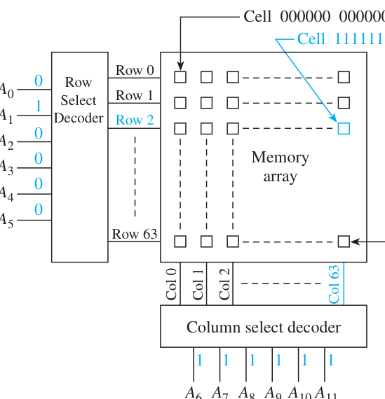
be input The storage locations are set up as a 64 * 64 array with A0 to location to be used. The data sheet for the 2147H is given in Figure 16–5(a). This figure shows the row and column circuitry used to pinpoint the memory cell within the
64 * 64 array. The box labeled “Row Select” is actually a 6-to-64 decoder for identidecoder for identifying the appropriate 1-of-64 column.
2147H memory array are pinpointed. The Row Select Decoder uses the lower address lines (A5 to A0) to develop a single active-HIGH line based on their binary value. For
example, if A5 to A0 = 000010, then ROW 2 will be HIGH. Then, to pinpoint the determine which of the 64 possible columns should be active-HIGH. For example, if the complete 12-bit address (A11 to A0) is 111111 000010, we will be accessing the memory cell that is in row 2, column 63, as illustrated in Figure 16–5(b). Once the location is selected, the AND gates at the bottom of the block diagram allow the data bit to either pass into (Din) or come out of (Dout) the memory location selected. Each memory location, or cell, is actually a configuration of transistors that functions like a flip-flop that can be Set (1) or Reset (0). (a) Team Discussion
(b)
Figure 16–5 The 2147H 4K * 1 static RAM: (a) Data sheet; (b) address row and column
decoders select memory cell 111111 000010 in the 2147H memory array;
(c)
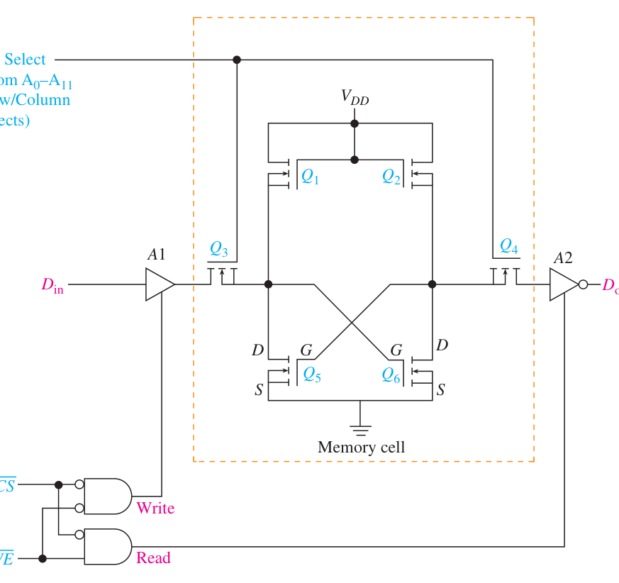
Figure 16–5 (Continued ) (c) functional diagram of a single cell within the static RAM
memory array. [(a) Courtesy of Intel Corporation.] During write operations, for Din to pass through its three-state buffer, the Chip
| Select | (CS) | must be LOW and the Write Enable | (WE) | must also be LOW. During read |
|---|---|---|---|---|
| operations, for Dout to receive data from its three-state buffer, the Chip Select | (CS) | must be LOW and the Write Enable | (WE) | must be HIGH, signifying a read operation. |
Figure 16–5(c) shows the internal configuration of a single cell of an SRAM
memory like the 2147H. All transistors are N-channel MOSFETs (Metal Oxide Semiconductor Field-Effect Transistor), which, as you may remember, turn ON (become a short) when a positive voltage (a logic 1) is placed on its gate. (See Section 9–5 for a review of MOSFETs.) A1 and A2 are three-state buffers used to enable a data bit
to be written into the memory cell if WE = 0 or read from the memory cell if WE = 1. coded into a single row and column in such a way to place a HIGH on the internal memory array line labeled bit select. This HIGH turns on Q3 and Q4, which allow the data to enter (or leave) the cross-connection circuit (Q5 and Q6) that holds the data bit.
To store a 1 into the memory cell, Din is made HIGH, and CS and WE are made sistor essentially acts like a short, placing 0 V (0) at the drain of Q6, which also places 0 V at the gate of Q5, turning it off. Because Q5 is OFF, its drain voltage will be close to VDD (1). Q1 and Q2 are used to provide the bias for the memory transistors, Q5 and Q6. Now that the data are loaded into the cell, this bit select line can go LOW, allowing the 2147H to access another cell. This isolates this memory cell from the outside world by turning Q3 and Q4 OFF. As long as VDD is still applied, the 1 that was loaded into the cell will remain there in the form of an ON Q6, which holds Q5 in an OFF state, which in turn holds Q6 in an ON state similar to the cross-NAND S-R flip-flop. The need to maintain a VDD supply voltage makes this a volatile memory. If VDD is turned off, no one could predict what state Q5 and Q6 will return to when power is reapplied.
on when you inadvertently hit the power switch on your PC.)
To read data out of the memory cell, CS is made LOW and WE is made HIGH, on bit select, the value on Q6 will be inverted and passed out to Dout as the original level that was input at Din. The timing waveforms for the Read and Write cycles are given in Figure 16–6.
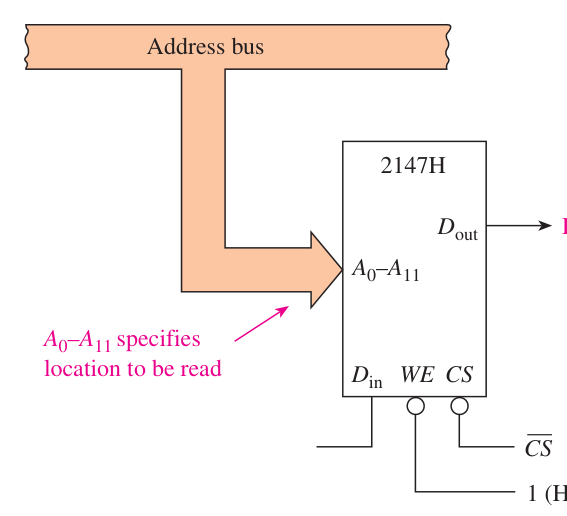
Read Operation: The circuit connections and waveforms for reading data from a
from the address bus for address selection. The WE input is held HIGH to enable the Referring to the timing diagram, when the new address is entered in the A0 to A11
inputs and the CS line goes LOW, it takes a short period of time, called the access time,
tRC tAA
A0–A11 New address
| High impedance | High impedance | |
|---|---|---|
| Dout | Undetermined | Data valid |
tACS tHZ
| Symbol | Parameter | Min. | Max. | Unit |
|---|---|---|---|---|
| tRC | Read cycle time tAA tACS | 35 Address access time Chip select access time | ns 35 35 | ns ns |
| tHZ | Chip deselection to high-Z out | 0 | 30 | ns |
(a)
Figure 16–6 The 2147H static RAM timing waveforms: (a) Read cycle;
tWC
A0–A11 New address
| CS | tDH | |||
|---|---|---|---|---|
| Din | Don’t care | Data in valid | ||
| Symbol | Parameter | Min. | Max. | Unit |
| tWC | Write cycle time | 35 | ns | |
| tDW | Data valid to end of write (Setup) | 20 | ns | |
| tDH | Data hold | 0 | ns |
(b)
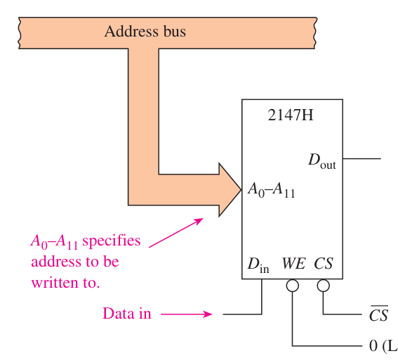
Figure 16–6 (Continued ) (b) Write cycle.
| of the Read cycle to the end of tACS, or tAA, whichever ends last. Before the | CS | is |
|---|---|---|
| brought LOW, Dout is in a high-impedance (float) state. The | CS | and A0 to A11 inputs |
must both be held stable for a minimum length of time, tRC, before another Read cycle can be initiated.
After CS goes back HIGH, the data out is still valid for a short period of time, tHZ,
| Write Operation: | A similar set of waveforms is used for the Write operation [Figure | |||
|---|---|---|---|---|
| 16–6(b)]. In this case, the Din is written into memory while the | CS | and | WE | are both LOW. |
| The Din must be set up for a length of time before either | CS | or | WE | go back HIGH (tDW), |
| and it must also be held for a length of time after either | CS | or | WE | go back HIGH (tDH). |
| Memory Expansion: | Because the contents of each memory location in the 2147H is |
only 1 bit, to be used in an 8-bit computer system, eight 2147Hs must be set up in such a way that, when an address is specified, 8 bits of data will be read or written. With eight
2147s, we have a 4096 * 8(4K * 8) memory system, as shown in Figure 16–7(a). are all connected to the same address bus lines. This way, when reading or writing from
| Dout | Din | CS |
|---|---|---|
| A0–A11 | 2147H |
WE D6
| Dout | Din | CS | and (b) thirty-two 2114s configured as two banks of 8K * 8. |
|---|---|---|---|
| A0–A11 | 2147H |
WE D5
| Dout | Din | CS |
|---|---|---|
| A0–A11 | 2147H |
WE D4
| Dout | Din | CS |
|---|---|---|
| A0–A11 | 2147H |
Address bus (A0–A11) WE
| D3 | (a) | (b) |
|---|---|---|
| Data bus (D0–D7) | 4K * 8 | |
| Dout | Din A0–A11 | CS 2147H |
RAM memory expansion: (a) eight 2147Hs configured as a WE D2
| Dout | Din | CS |
|---|---|---|
| A0–A11 | 2147H |
WE D1
| data bus simultaneously. The | WE | input determines which internal three-state buffer is |
|---|---|---|
| enabled, connecting either Din or Dout to the data bus. The | WE | input is sometimes la- |
| beled | READ/WRITE, | meaning that it is HIGH for a Read operation, which puts data |
out to the data bus via Dout, and it is LOW for a Write operation, which writes data into the memory via Din. Several other configurations of RAM memory are available. For example, the
| 2114 is configured as a | 1024 * 4@bit | (1K * 4) | RAM instead of the | 4096 * 1 | used by |
|---|---|---|---|---|---|
| the 2147H. A | 1024 * 4@bit | RAM will input/output 4 bits at a time for each address |
specified. This way, interfacing to an 8-bit data bus is simplified by having to use only two 2114s, one for the LOW-order data bits (D0 to D3) and the other for the HIGH-order data bits (D4 to D7). For example, the photograph in Figure 16–7(b) shows a memory expansion printed-circuit board with thirty-two 2114 RAM ICs. They are set up as two
memory banks, each configured as 8K * 8. learn the fundamentals of static RAM circuitry, but it will never find its way into new designs. Much faster, denser, lower-power SRAMs are available for the digital designer. For example, modern SRAMs have bit densities ranging from 64 kb (kilobit) to
4 Mb and access speeds as fast as 7.5 ns. Power demand is as low as 3.3mW when in
chip by making CS = HIGH. Examples for a few SRAM memory configurations for
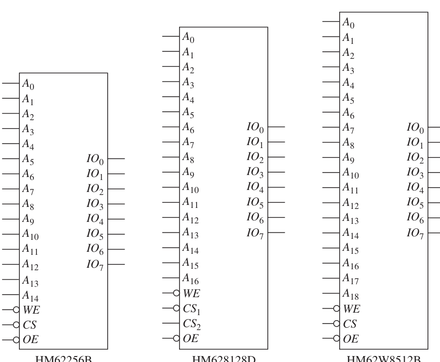
Figure 16–8 Logic symbols for several Hitachi low-power SRAMs.
| TABLE 16–1 | Sample Hitachi Low-Power Static RAMs | |
|---|---|---|
| Part No. | Density | Configuration |
| HM6264B | 64 kb | 8k �8 |
| HM62256B | 256 kb | 32k �8 |
| HM628128D | 1 Mb | 128k �8 |
| HM62W8512B | 4 Mb | 512k �8 |
small, but if your application only calls for that much memory, you can save a lot of space on your circuit board because it is only a 28-pin IC. It is available as a throughhole DIP or as a surface-mount SOP28 package. On the other end of the spectrum, the HM62W8512B is a 4-Mb SRAM config-
ured as 512k * 8. To access 512k memory locations, we need 19 address lines (A0
| to A18), as shown in Figure 16–8 | As you can see in the logic symbol, it | ||
|---|---|---|---|
| has 8 I/O lines. It is written to by making | WE = LOW | and read from by making | |
| WE = HIGH. | A LOW | CS | performs a chip select to access memory, and a HIGH puts |
| it in standby mode, reducing its power consumption to | 3.3mW | (typical). Several of the | |
| higher-end SRAMs such as this are made to operate with | VCC = 3.3V, | making it com- |
patible with the low-voltage families such as LV-TTL. It is available in 32-pin surfacemount package styles only. A list of the Web sites for Hitachi and other memory manufacturers is given in Appendix A.
Review Questions
16–6. The 2114 memory IC is a 1K * 4 static RAM, which means that it has
16–7. To perform a read operation with a 2147H RAM, CS must be
__________ (LOW/HIGH) and WE must be __________ (LOW/HIGH). __________ are used to select the row, and __________ through __________ are used to select the column. 16–9. In Figure 16–5(b), what is the row and column selected if the address (A11 to A0) is 001001000111? 16–10. Which transistor(s) in Figure 16–5(c) store the memory bit? 16–11. According to the Read cycle timing waveforms for the 2147H, how
long must you wait after a chip select (CS) before valid data are available
16–3 Dynamic RAMs
Although dynamic RAMs (DRAMs) require more support circuitry and are more difficult to use than static RAMs (SRAMs), they are less expensive per bit and have a much higher density, minimizing circuit-board area. Most applications requiring large amounts of read/write memory will use DRAMs instead of static. The main memory in PCs use 2, 4, 8, or more gigabytes of DRAM. The most important difference in a DRAM memory is that its storage technique is to place a charge on a capacitor inside each memory location instead of using the crosstransistor configuration of SRAMs. Using this method greatly reduces the size per bit. However, the time it takes to read or write a bit is greater for the DRAM because it has to change the charge on the capacitor, which takes longer than changing the state of the MOS transistors in the SRAM.
Figure 16–9 shows a simplified schematic of a single DRAM memory cell. The
storage capacitor is isolated from the Din or Dout line until the MOSFET control transistor is turned ON momentarily with a write or read pulse at its gate. To write a 1 to
the capacitor, Din is set to 1 (+VCC), and the DRAM control circuitry provides a pulse
| MOSFET | MOSFET | ||
|---|---|---|---|
| Write | control | Read | control |
| pulse | transistor | pulse | transistor |
| Storage | + | Storage |
VCC
| capacitor | − | capacitor |
|---|---|---|
| (a) | (b) Figure 16–9 | Simplified DRAM memory cell: (a) writing a 1 to the storage capacitor and |
(b) reading a 1 from the storage capacitor. to the gate of the selected memory cell. This pulse turns the transistor ON, shorting the
| drain to source and placing | +VCC | on the capacitor. (Depending on the DRAM family, | |||
|---|---|---|---|---|---|
| +VCC | will be | +5 | or | +3.3V, | and in some cases even lower.) To read the data at the cell |
location, the DRAM control circuitry redirects the drain of the MOSFET to the Dout line and issues a read pulse on its gate. This shorts the transistor, connecting the capacitor directly to Dout. As you know, capacitors cannot hold their charge forever, even when the MOSFET control transistor is an open. Therefore, the capacitor has to be refreshed on a regular basis, called the refresh period. The refresh period for the earlier DRAMs like the 2118 was 2 ms, but newer technology has extended the period to 64 ms. Figure 16–10 shows the voltage on a storage capacitor that is initially 0 V, then loaded with a 1
(+VCC). The voltage, +VCC, will immediately start dropping and require refreshing Refresh period +VCC Vcapacitor
| 0 V | Time | |
|---|---|---|
| Figure 16–10 | Refreshing the voltage on the DRAM storage capacitor. | |
| An example of a | 16K * 1 | -bit DRAM is the Intel 2118, whose data sheet is |
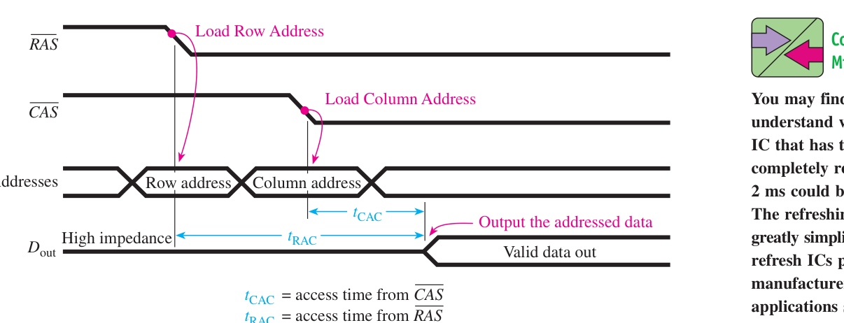
shown in Figure 16–11(a). (214= 16,384). To uniquely address 16,384 locations, 14 address lines are required However, Figure 16–11(a) shows only seven address lines (A0 to A6). This is because with larger memories such as this, to keep the IC pin count to a minimum, the address lines are multiplexed into two groups of seven. An external 14-line-to-7-line multi-
plexer is required in conjunction with the control signals, RAS and CAS, to access a The controlling device must put the valid 7-bit address of the desired memory
array row on the A0 to A6 inputs and then send the Row Address Strobe (RAS) LOW. ray column on the same A0 to A6 inputs and then send the Column Address Strobe
(CAS) LOW. Each of these 7-bit addresses is latched and will pinpoint the desired 1-bit
(a)
(b) for a PC are practically
(c)
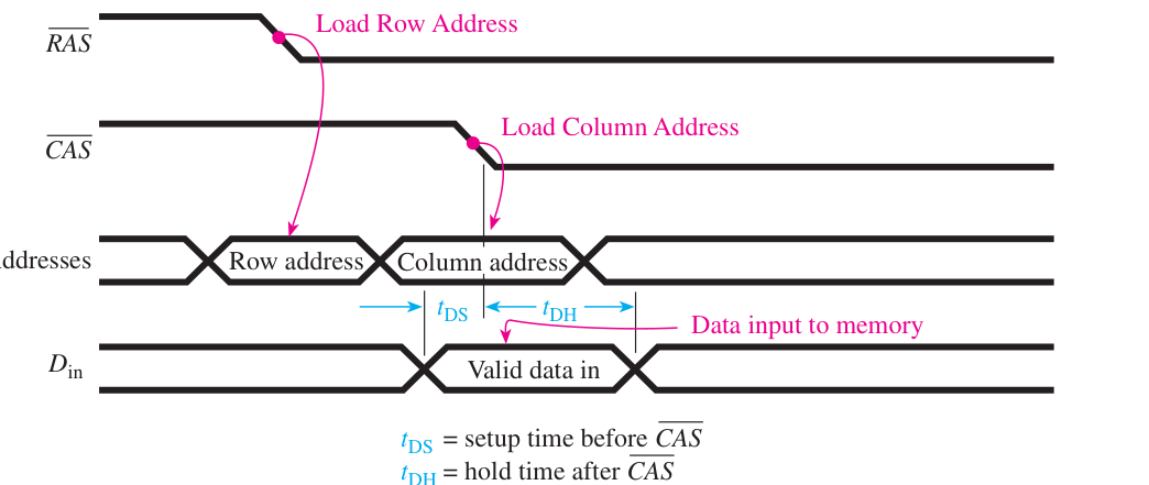
Figure 16–11 (a) The 2118 16K * 1 dynamic RAM; (b) dynamic RAM Read cycle timing
(WE = HIGH) ; (c) dynamic RAM Write cycle timing (WE = LOW). [(a) Courtesy of Intel
Once the memory location is identified, the WE input is used to direct either a
When WE is LOW, data are written to the RAM via Din; when WE is HIGH, data are
- 1. WE is HIGH.
- 2. A0 to A6 are set up with the row address, and RAS is sent LOW.
- 3. A0 to A6 are set up with the column address, and CAS is sent LOW.
- 4. After the access time from RAS or CAS (whichever is longer), the Dout line
will contain valid data.
Write Cycle Timing [Figure 16–11(c)]
- 1. WE is LOW.
- 2. A0 to A6 are set up with the row address, and RAS is sent LOW.
- 3. A0 to A6 are set up with the column address, and CAS is sent low.
- 4. At the HIGH-to-LOW edge of CAS, the level at Din is stored at the specified
row–column memory address. Din must be set up before and held after the
HIGH-to-LOW edge of CAS to be interpreted correctly. (There are other for more complete specifications.)
Refresh Cycle Timing
Each of the 128 rows of the 2118 must be refreshed every 2 ms or sooner to replenish the charge on the internal capacitors. There are three ways to refresh the memory cells:
1. Read cycle
2. Write cycle
3. RAS -only cycle
| Unless you are reading or writing from all 128 rows every 2 ms, the | RAS | -only |
|---|---|---|
| cycle is the preferred technique to provide data retention. To perform a | RAS | -only cycle, |
the following procedure is used:
- 1. CAS is HIGH.
- 2. A0 to A6 are set up with the row address 000 0000.
- 3. RAS is pulsed LOW.
- 4. Increment the A0 to A6 row address by 1.
- 5. Repeat steps 3 and 4 until all 128 rows have been accessed.
Dynamic RAM Controllers
It seems like a lot of work demultiplexing the addresses and refreshing the memory cells, doesn’t it? Well, most manufacturers of DRAMs have developed controller ICs to simplify the task. Some of the newer dynamic RAMs have refresh and error detection/correction circuitry built right in, which makes the DRAM look static to the user. A popular controller IC to interface to the 2118 is the Intel 3242 address multiplexer and refresh counter for 16K dynamic RAMs. Figure 16–12 shows how this controller IC is used in conjunction with four 2118 DRAMs. The 3242 in Figure 16–12 is used to multiplex the 14 input addresses A0 to A13
| to seven active-LOW output addresses | Q0 | to | Q6. | When the Row Enable input is |
|---|---|---|---|---|
| HIGH, A0 to A6 are output inverted to | Q0 | to | Q6 | as the row addresses. When the Row |
| Enable input is LOW, A7 to A13 are output inverted to | Q0 | to | Q6 | as the column address. |
| Of course, the timing of the | RAS | and | CAS | on the 2118s must be synchronized with the |
Row Enable signal.
| 2118 | D0 |
|---|---|
| A0 | Din |
| ••• | Dout |
A6 RAS 3242
| Q0 | CAS |
|---|---|
| ••• | WE |
A0 ••• Q6 A13
| Dynamic | 2118 | D1 |
|---|---|---|
| RAM | A0 controller | Din ••• |
Dout Refresh
enable Zero A6
RAS Data bus CAS Count WE
| 2118 | D2 |
|---|---|
| A0 | Din |
| ••• | Dout |
A6 RAS CAS WE
| 2118 | D3 |
|---|---|
| A0 | Din |
| ••• | Dout |
A6 RAS CAS WE
Figure 16–12 Using a 3242 address multiplexer and refresh counter in a 16K * 4 dynamic
RAM memory system. To provide a “burst” refresh to all 128 rows of the 2118s, the Refresh Enable in-
| put in Figure 16–12 is made HIGH. This causes the | Q0 | to | Q6 | outputs to count from 0 |
|---|---|---|---|---|
| to 127 at a rate determined by the | count | input clock signal. When the first 6 significant bits of the counter sequence to all zeros, the | zero | output goes LOW, signifying the |
completion of the first 64 refresh cycles. Modern DRAMs have capacities in the megabyte range and, thus, need controllers with additional address lines. National Semiconductor DM8420 series provides control for 4, 16, or 64 MB of DRAM.
One commonly used method of setting up the timing for RAS,CAS, and Row
In
74S04 74S04 74S04 74S04
| To all RAS | 500 ns | ||
|---|---|---|---|
| 500 ns | In | T1 | To row enable |
| T2 | To all CAS | ||
| T3 | 100 ns |
100 ns T4 (b)
Figure 16–13 Four-tap, 50-ns delay line used for DRAM timing: (a) logic diagram and
(b) logic symbol and timing. delay line IC of Figure 16–13(a) is made up of four inverters with precision RCs to develop a 50-ns delay between each inverter. The pulses out of each tap have the same width, but each successive tap is inverted and delayed by 50 ns. [In Figure 16–13(b), every other tap was used to arrive at noninverted, 100-ns delay pulses.] Delay lines are Inside very useful for circuits requiring sequencing, as DRAM memory systems do. (See Your PC
Figure 11–16 for a 5-ns multitap delay gate.)
| Modern PCs use 2 GB, | The waveforms produced by the delay line of Figure 16–13(b) can be used to | ||||
|---|---|---|---|---|---|
| 4 GB, or more of DRAM. | drive the control inputs to the | 16K * 4 | dynamic RAM memory system of Figure | ||
| To physically mount so much | 16–12 (a LOW | RAS | pulse, then a LOW Row Enable pulse, then a LOW | CAS | pulse). |
| memory, manufacturers | Careful inspection of the data sheets for the 3242 and 2118 is required to determine |
solder several memory ICs the maximum and minimum allowable values for pulse widths and delay times. To on a single board, which is design the absolute fastest possible memory circuit, all the times would be kept at then inserted into a special their minimum value. But, it is a good practice to design in a 10% to 20% margin to socket on the motherboard.
| These memory boards are | be safe. |
|---|---|
| called SIMMs (Single- | Because of their extremely high circuit density, DRAMs are the choice for a PC’s |
| Inline Memory Modules), | large RAM requirement. Typical DRAM capacities for PCs are 64, 96, and 128 MB |
| DIMMs (Dual-Inline | and higher. Table 16–2 lists several popular high-density dynamic RAM ICs available |
| Memory Modules), or | from Hitachi Semiconductor. |
RIMMs (Rambus-Inline Memory Modules). As memory requirements increase, these memory
modules can easily be TABLE 16–2 Sample Hitachi Low-Power DRAMs
| without any special tools. | Part No. | Density | Configuration | Voltage |
|---|---|---|---|---|
| (For SIMM, DIMM, and | HM5165805 | 64 Mb | 8M * 8 | 3.3 V |
| RIMM availability, visit the | HM5113805 | 128 Mb | 16M * 8 | 3.3 V |
| DRAM manufacturers’ | HM5225805 | 256 Mb | 32M * 8 | 3.3 V |
| Web sites listed in | HM5251805 | 512 Mb | 64M * 8 | 3.3 V |
Appendix A.)
16–12. Why are address lines on larger memory ICs multiplexed? 16–13. What is the primary storage medium in a DRAM memory cell? 16–14. What is meant by refreshing a DRAM? 16–15. What is a typical refresh period for a DRAM (60 s/1 s/60 ms)?
16–4 Read-Only Memories
Read-Only Memories (ROMs) are memory ICs used to store data on a permanent basis. They are capable of random access and are nonvolatile, meaning that they do not lose their memory contents when power is removed. This makes them very useful for the storage of computer operating systems, software language compilers, table look-ups, specialized code conversion routines, and programs for dedicated microprocessor applications. ROMs are generally used for read-only operations and are not written to after they are initially programmed. However, there is an erasable variety of ROM called an EPROM (erasable-programmable-read-only memory) that is very useful because it can be erased and then reprogrammed if desired. To use a ROM, the user simply specifies the correct address to be read and then
enables the chip select (CS). The data contents at that address (usually 8 bits) will then
have to enable the output with a LOW on OE). Manufacturers will make a custom mask ROM for users who are absolutely sure of the desired contents of the ROM and have a need for at least 1000 chips. To fabricate a custom IC like the mask ROM, the manufacturer charges a one-time fee of more than $1000 for the design of a unique mask that is required in the fabrication of the IC. After that, each identical ROM that is produced is very inexpensive. In basic terms, a mask is a cover placed over the silicon chip during fabrication that determines the permanent logic state to be formed at each memory location. Of course, before the mass production of a quantity of mask ROMs, the user should have thoroughly tested the program or data that will be used as the model for the mask. Most desktop computers use mask ROMs to contain their operating system and for executing procedures that do not change, such as decoding the keyboard and the generation of characters for the display. Figure 16–14 shows how a 1 or 0 is derived when the IC manufacturer alters the source connection of a single MOSFET.
| VDD | VDD |
|---|---|
| R | R |
| Dout= 1 | Dout= 0 |
| D | D |
| Bit | Bit |
| G | G |
| select | select |
| S | S |
| Source open | Source connected |
| from ground | to ground |
| (a) Fabricated with an open | (b) Fabricated with a source shorted |
| source to yield Dout= 1 | to ground to yield Dout= 0 |
| Figure 16–14 | Simplified schematic of a single mask-ROM memory cell. |
To avoid the high one-time cost of producing a custom mask, IC manufacturers provide user-programmable ROMs (PROMs). They are available in standard configura-
tions such as 4K * 4,4K * 8,8K * 4, and so on. 16–15). A 0 is changed to a 1 by sending a high-enough current through the fuse to permanently open it, making the output of that cell a 1. The programming procedure involves addressing each memory location, in turn, and placing the 4- or 8-bit data to be programmed at the PROM outputs and then applying a programming pulse (either a HIGH voltage or a constant current to the programming pin). Details for programming are given in the next section.
VDD VDD
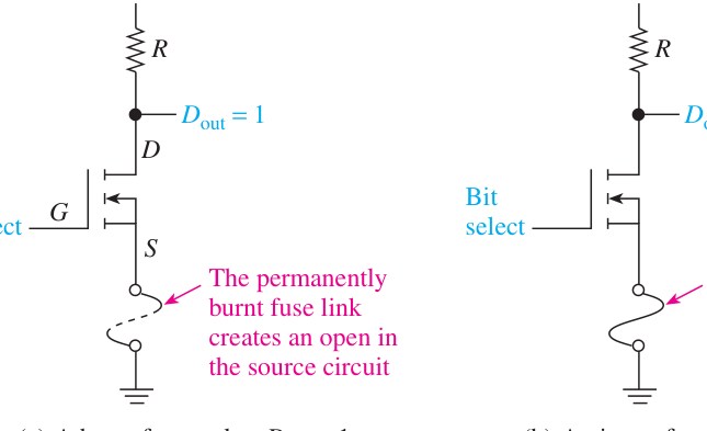
Figure 16–15 Simplified schematic of a single fusible-link PROM memory cell.
Once the fusible link is burned open, the data are permanently stored in the PROM and can be read over and over again just by accessing the correct memory address. The process of programming such a large number of locations is best done by a PROM programmer or microprocessor development system (MDS). These systems can copy a good PROM or the data can be input via a computer keyboard or from a magnetic disk.
EPROMs, EEPROMs, and Flash Memory
When using mask ROMs or PROMs, if you need to make a change in the memory contents or if you make a mistake in the initial programming, you are out of luck! One solution to that problem is to use an erasable PROM (EPROM). These PROMs are erased by exposing an open “window” (See Figure 16–16) in the IC to an ultraviolet (UV) light source for a specified length of time. Two other types of EPROMs are the Electrically Erasable PROM (EEPROM) and Flash memory. The EEPROM provides nonvolatile memory but can be programmed and erased while still in the circuit. Like the EEPROM, Flash memory is also electrically erasable. It derives its name from the fact that its internal processing capability provides for much faster access times and reduced system overhead during the erasure process. Any of these three memories can be erased and reprogrammed thousands of times reliably. There is, however, one type of EPROM having a part number suffix-OTP, which stands for One-Time-Programmable. Because it is only programmed once, it is used like a PROM but has pin compatibility and I/O specs the same as its EPROM part number. The UV-erasable EPROM has the slowest erasure time. It takes several minutes of intense UV radiation, and you have no choice but to erase the entire chip. The EEPROMs and Flash memory are more flexible, allowing for individual bits or bytes to be erased in less than a millisecond. Flash memory even goes one step further, allowing you to erase entire blocks or the entire chip in the same time that it takes an EEPROM to erase 1 byte.
Figure 16–16 A 2716 EPROM IC showing the window that allows UV light to strike the
memory cells for erasure. The UV-erasable EPROMs are the least expensive and are generally used during the initial design and debug stages of new product implementation. Designers will program their initial versions of software and data on an EPROM to test their ideas. Once a series of tests and retests have been passed, they will order the mask ROM version or implement the design with an FPGA or EEPROM-type device. Commercially available EPROM programmers usually connect to a PC. A blank EPROM is plugged into a socket on the programmer, and then a command is given to the PC to download the binary program or data bytes that the designer wants put on the EPROM. An opaque cover is then placed over the exposed window to avoid inadvertent erasure, which can be caused by sunlight or fluorescent lighting. To erase the EPROM, the opaque cover is removed, and the IC is placed in a UV eraser device, which bombards the open EPROM window with UV radiation for a specified length of time (usually several minutes). Because of their in-circuit reprogrammability, EEPROMs are becoming more popular than EPROMs. EEPROMs are often sold as serial I/O memory devices. This significantly cuts down on their pin count and chip size. Their reduced size makes them a perfect solution for handheld devices like TV remote controls to remember favorite user settings and in cell phones for last-number radial and speed dial. Flash memory has become the most popular nonvolatile memory solution for
many of the new electronic devices recently introduced. Digital cameras and personal digital assistants (PDAs) use Flash cards as their medium to store data. Also, PCs store operating system firmware, and printers store fonts on Flash memory. The most common device used for individual memory cells for each of these three nonvolatile memories is the floating-gate MOSFET, as shown in Figure 16–17. The floating gate is the actual storage element for these devices. It is insulated from the three transistor connections by a dielectric layer on one side and by a thin oxide layer on the other. By placing a high-enough voltage at the control gate, an electric-field effect is created across the floating gate, which forces it to gain an excess of electrons.
(storage element) Control gate Dielectric
layer Source oxide layer
Figure 16–17 Floating-gate MOSFET.
Manufacturers guarantee that this electron charge will remain on the floating gate for more than 10 years unless drained off by electrically erasing the cell. So, basically we need to perform three operations on this memory cell: write, erase, and read. Figure 16–18(a) shows how a 1 is written to a cell. Internal chip circuitry places a high voltage (usually 12 V), called VPP, on the control gate and connects the transistor source to ground. This creates an extremely high electric field across the floating gate. The floating gate responds by absorbing electrons that jump across the thin oxide layer from the transistor source. This continues for a few nanoseconds, until a sufficient charge is obtained. When the VPP voltage is removed,
VCC N.C. (no connection)
| Your PC | R | R |
|---|---|---|
| Floating gate | Floating gate | |
| Digital cameras and smart | D | D |
| phones, etc. use Flash mem- | e− | e− |
Control
| ory cards as their medium | e− | Control | e− |
|---|---|---|---|
| gate | e− | e− | |
| to store data. | e− | gate | e− |
VPP
| e− | e− |
|---|---|
| e− | e− |
| e− | e− |
| S | e− |
| e− | S |
VPP
(a) Writing a 1 to a cell (b) Erasing a cell to a 0
VCC VCC with electron
| R | R | ||
|---|---|---|---|
| Floating gate | charge raises | ||
| with no charge | D | ON threshold | D |
| Dout= 0 | Dout= 1 | ||
| Control | Control | e− |
e−
| gate | ON | gate | e− | OFF |
|---|---|---|---|---|
| VCC | VCC (c) | e− Reading an erased cell | S (d) Figure 16–18 | S Reading a written cell Simplified diagram of the memory cell used for EPROMs, EEPROMs, and |
Flash memories.
tric and oxide layers. To erase the memory cell of an EEPROM or Flash memory, the electrons must be drained off the floating gate, as shown in Figure 16–18(b). To do this, the internal control circuitry reverses the connections to the control gate and source, reversing the write operation and leaving the floating gate empty of excess electrons. (A UV-erasable EPROM has the excess electrons removed when it absorbs UV light energy through its open window.) To read a cell, the address lines connected to the memory IC are decoded into a specific row and column to select a particular memory cell within the memory array, as was done with RAM ICs. This causes the bit-select line to place VCC on the control gate of the selected memory cell, as shown in Figures 16–18(c) and 16–18(d). If the floating gate has no electron charge on it [Figure 16–18(c)], the VCC voltage (usually 5 or 3.3 V) is sufficient to turn the transistor ON, but not high enough to add an electron charge to the floating gate. The ON transistor shorts the drain to source, which places 0 V at Dout. If the floating gate has a charge on it [Figure 16–18(d)], the VCC voltage will not be high enough to overcome the threshold required to turn the transistor ON. An OFF transistor acts like an open, keeping the current flow to zero and making the
drain voltage equal to VCC, so Dout = 1. EPROM ICs. A sample of the interface circuitry and timing for a small EPROM, the 2716, is given in Figure 16–19.
The 2716 EPROM: The data sheet for the 2716 EPROM is given in Appendix B. Re(211= 2048),
2k * 8 = 2k locations that require 11 address inputs which are labeled To read a byte (8 bits) of data from the chip, the 11 address lines are set up, and
then CE and OE are brought LOW to enable the chip and to enable the output. The timtime delay for setting up the addresses (tACC), enabling the chip (tCE), or enabling the output (tOE), whichever is completed last. Figure 16–19(a) shows the circuit connections and waveforms for reading the 2716 EPROM. In Figure 16–19(a), the X in the address waveform signifies the point where the
address lines must change (1 to 0 or 0 to 1), if they are going to change. The CE/PGM
in the high-impedance state (float) until OE goes LOW. The outputs are then undeterfrom the addressed memory contents.
Programming the 2716: Initially, and after an erasure, all bits in the 2716 are 1s. To
- 1. Set VPP to 25 V and OE = HIGH(5V).
- 2. Set up the address of the byte location to be programmed.
- 3. Set up the 8-bit data to be programmed on the O0 to O7 outputs.
- 4. Apply a 50-ms positive TTL pulse to the CE/PGM input.
- 5. Repeat steps 2, 3, and 4 until all the desired locations have been pro-
grammed.
Figure 16–19(b) shows the circuit connections and waveforms for programming
a 2716.
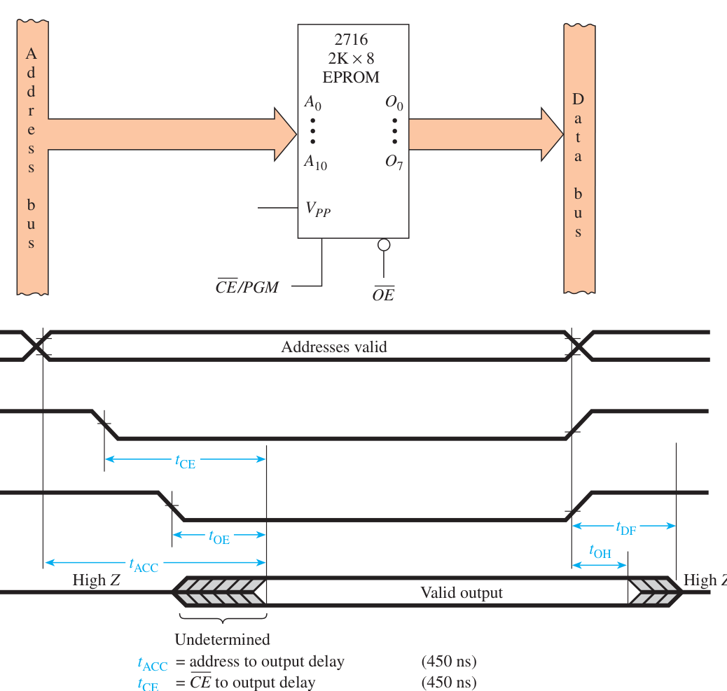
| tOE | = OE to output delay | (120 ns) |
|---|---|---|
| tDF | = OE HIGH to output float | (100 ns) |
| tOH | = output hold | (0 ns) |
(a)
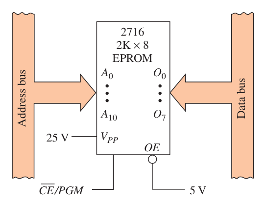
| Addresses | Addresses valid |
|---|---|
| Data | Data in valid |
| tDS | tDH |
| CE/PGM | Programming |
pulse
| tAS | 50 ms | tAH |
|---|---|---|
| tAS | = address setup time (2 μs min.) tDS tAH | = data setup time (2 μs min.) = address hold time (2 μs min.) |
| (b) | tDH Figure 16–19 | = data hold time (2 μs min.) The 2716 EPROM: (a) Read cycle; (b) Program cycle. |
memory available today. In general, EEPROMs have the smallest bit size, and the Flash memory has the largest. Flash memory is the fastest-growing family of this type, finding applications in many PCs and other consumer electronic devices. Flash memory is now packaged in modules (Flash cards) that can be handled by consumers as they insert it into a slot or USB port on their PC or handheld device. Flash cards can have densities exceeding 256 gigabytes.
| TABLE 16–3 | Representative EPROMs, EEPROMs, and Flash Memory | |
|---|---|---|
| Part Number | Organization | Description |
| 27C16 | 2k * 8 | 16k UV-Erasable CMOS EPROM |
| 27C256 | 32k * 8 | 256k UV-Erasable CMOS EPROM |
| 27C040 | 512k * 8 | 4Meg UV-Erasable CMOS EPROM |
| 28C64 | 8k * 8 | 64k CMOS EEPROM |
| 24C64 | 8k * 8 | 64k Serial CMOS EEPROM |
| 24C256 | 32k * 8 | 256k Serial CMOS EEPROM |
| 29F080 | 1M * 8 | 8Meg CMOS Flash Memory |
| 29F032 | 4M * 8 | 32Meg CMOS Flash Memory |
| 29W25611 | 32M * 8 | 256Meg CMOS Flash Memory |
Table 16–4 summarizes all of the semiconductor memories.
| TABLE 16–4 | Summary of Semiconductor Memory | ||||
|---|---|---|---|---|---|
| Memory | Basic Cell | In-Circuit | |||
| Type | Structure | Volatile | Rewriteable | Density | Comments |
| SRAM | Cross-connected | Yes | Yes | Low | Fastest speed makes them well suited |
| MOSFETs | for PC cache memory. | ||||
| DRAM | MOSFET with | Yes | Yes | High | Slower than SRAM, but extremely high |
| capacitor | density. Used for PC main RAM memory. | ||||
| Mask ROM | MOSFET | No | No | High | High initial cost, but useful for high |
production runs such as PC BIOS.
| PROM | MOSFET with | No | No | High | Program once; used for small-volume |
|---|---|---|---|---|---|
| fused link | or trial circuits and data tables. | ||||
| EPROM | Floating-gate | No | No | High MOSFET | Slow erasure time, but very high density and fast access time. Used for initial |
troubleshooting and design.
| EEPROM | Floating-gate | No | Yes | Low | Small size and ability to rewrite make |
|---|---|---|---|---|---|
| MOSFET | it useful for handheld portable electronic |
devices.
| Flash | Floating-gate | No | Yes | High | Extremely high density and ability to |
|---|---|---|---|---|---|
| MOSFET | rewrite facilitate portable megabyte |
memory like the Flash card.
16–16. What is meant by the term volatile? 16–17. Describe a situation where you would want to convert your EPROM memory design over to the mask ROMs. 16–18. Describe how a memory cell in each of the following memories is made to output a 1: (a) mask ROM (b) PROM (c) EPROM (d) EEPROM (e) Flash memory 16–19. Describe how you erase a memory cell in each of the following memories: (a) EPROM (b) EEPROM (c) Flash memory 16–20. According to the 2716 EPROM Read cycle timing waveforms, you
| must wait ________ nanoseconds after | OE | goes LOW before the data at O0 |
|---|---|---|
| to O7 are valid (assuming | CE | has already been LOW for at least ________ |
nanosecond). 16–21. The time for the outputs to return to a float state for the 2716 is
tDF = 100ns. Under what circumstances would that time be important to
16–5 Memory Expansion and Address
Decoding Applications
When more than one memory IC is used in a circuit, a decoding technique (called address decoding) must be used to identify which IC is to be read or written to. Most 8-bit microprocessors use 16 separate address lines to identify unique addresses within the computer system. Some of those 16 lines will be used to identify the chip to be accessed, whereas the others pinpoint the exact memory location. For instance, the 2732
is a 4K * 8 EPROM that requires 12 of these address lines (A0 to A11) just to locate chip address decoding. A12 to A15 can be used to identify which IC within the system is to be accessed. (216= 65,536),
With 16 total address lines, there will be 64K, or 65,536 unique ory system, let’s say, 16K bytes, four 2732s would be required. The address decoding scheme shown in Figure 16–20 could be used to set up the four EPROMS consecutively in the first 16K addresses of a computer system. The four EPROMs in Figure 16–20 are set up in consecutive memory locations between 0 and 16K and are individually enabled by the 74LS138 address decoder.
The 4K * 8 EPROMs each require 12 address lines for internal memory selection, the 74LS138.
| A14 | A13 A12 | A15 |
|---|---|---|
| A0–A11 | A0–A15 (12) | (16) |
Data from selected EPROM
A0–A15 Microprocessor D0–D7 (8) Microprocessor issues LOW Read pulse 2732 (4K × 8)
A0–A11 ADDR 0000-0FFF D0–D7 (8)
| CE | OE |
|---|---|
| EN1 | 0 |
A15
| EN2 | 1 | |
|---|---|---|
| 1 | EN3 | 2 |
| 2732 (4K × 8) | 8-Bit data bus | |
| 3 | ADDR 1000-1FFF | |
| A0–A11 | D0–D7 | (8) |
| 4 | (4K–8K) | |
| A12 | CE | OE |
| A0 | 5 |
A13
A1 6
A2 7
| 1-of-8 | 2732 (4K × 8) | ||
|---|---|---|---|
| address | ADDR 2000-2FFF | ||
| decoder | A0–A11 | D0–D7 | (8) |
(8K–12K)
CE OE
A0–A11 ADDR 3000-3FFF D0–D7 (8)
Must be LOW CE OE Selects
| EPROM | Select location within EPROM | ||
|---|---|---|---|
| 0 | A2 | A1 A0 | D0–D7 outputs |
float unless
A15 A14 A13 A12 A11 A10 A9 A8 A7 A6 A5 A4 A3 A2 A1 A0
| Address decoder | Used by 2732 EPROMS |
|---|---|
| device selection | (0000 0000 0000 to |
| (0000 to 0011) | 1111 1111 1111) |
| Figure 16–20 | Address decoding scheme for a 16K-byte EPROM memory system. |
the unique 16-bit address that it wants to read from. Then it issues a LOW level on its
RD output. This satisfies the three enable inputs for the 74LS138, which then uses A12, EPROMs. Once an EPROM has been selected, it outputs its addressed 8-bit contents
to the data bus. The outputs of the other EPROMs will float because their CE s are that it requested from the data bus.
| Team | The address decoding scheme shown in Figure 16–20 is a very common tech- |
|---|---|
| Discussion | nique used for mapping out the memory allocations in microprocessor-based sys- |
tems (called memory mapping). RAM (or RWM) is added to the memory system the This is a very popular same way.
| scheme for address decod- | 4K * 8 |
|---|---|
| For example, if we wanted to add four | RAMs, their chip enables would |
ing (Figure 16–20). To be be connected to the 4–5–6–7 outputs of the 74LS138, and they would occupy locasure that you thoroughly
| understand it, determine | tions 4XXX, 5XXX, 6XXX, and 7XXX. Then, when the microprocessor issues a |
|---|---|
| the new addresses if A15 is | Read or Write command for, let’s say, address 4007H (4007 Hex), the first RAM |
| moved to the EN3 input. | would be accessed. |
EXAMPLE 16–1
Determine which EPROM and which EPROM address are accessed when the microprocessor of Figure 16–20 issues a Read command for the following hex addresses: (a) READ 0007H; (b) READ 26C4H; (c) READ 3FFFH; (d) READ 5007H.
Solution:
(a) The HIGH-order hex digit (0) will select the first EPROM. Address 007 (0000 0000 0111) in the first EPROM will be accessed. (Address 007H is actually the eighth location in that EPROM.)
| (b) The HIGH-order hex digit (2) will select the third EPROM | (A15 = 0, |
|---|---|
| A14 = 0,A13 = 1,A12 = 0). | Address 6C4H in the third EPROM will |
be accessed.
| (c) The HIGH-order hex digit (3) will select the fourth EPROM | (A15 = 0, |
|---|---|
| A14 = 0,A13 = 1,A12 = 1). | Address FFFH (the last location) in the |
fourth EPROM will be accessed. (d) The HIGH-order hex digit (5) will cause the output 5 of the 74LS138 to go LOW. Because no EPROM is connected to it, nothing will be read.
Expansion to 64K
The memory system of Figure 16–20 can be expanded to 64K bytes by utilizing two 74LS138 decoders, as shown in Figure 16–21. Address lines A0 to A11 are not shown in Figure 16–21, but they would go to each 2732 EPROM, just as they did in Figure 16–20. The HIGH-order addresses (A12 to A15) are used to select the individual EPROMs. When A15 is LOW, the upper decoder in Figure 16–21 is enabled and EPROMs 1 to 8 can be selected. When A15 is HIGH, the lower decoder is enabled, and EPROMs 9 to 16 can be selected. Using the circuit in Figure 16–21 will allow us to map in six-
teen 4K * 8 EPROMs, which will completely fill the memory map in a 16-bit address RAM and I/O devices.
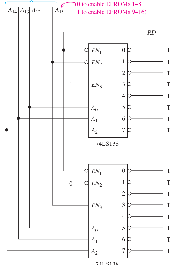
Figure 16–21 Expanding the memory of Figure 16–20 to 64K bytes.
One final point on memory and bus operation: Microprocessors and MOS memory ICs are generally designed to drive only a single TTL load. Therefore, when several inputs are being fed from the same bus, an MOS device driving the bus must be buffered. An octal buffer IC such as the 74244 connected between an MOS IC output and the data bus will provide the current capability to drive a heavily loaded data bus. Bidirectional bus drivers (or transceivers) such as the 74LS640 provide buffering in both directions for use by read/write memories (RAM or RWM).
APPLICATION 16–1
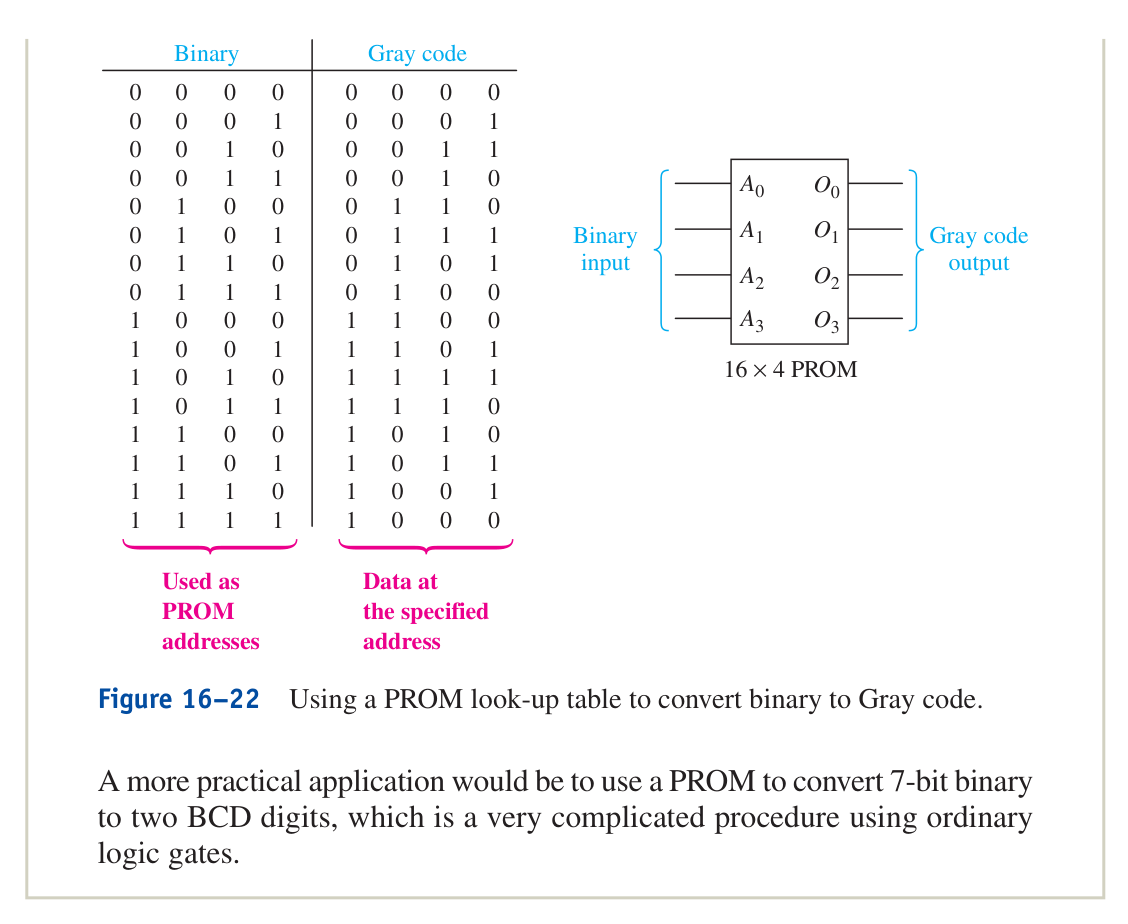
A PROM Look-Up Table
In addition to being used strictly for memory, ROMs, PROMs, and EPROMS can also be programmed to provide special-purpose functions. One common use is as a look-up table. A simple example is to use a PROM as a 4-bit binary-to-Gray code converter, as shown in Figure 16–22. The PROM chosen for Figure 16–22 must have 16 memory locations, each location containing a 4-bit Gray code. The 4-bit binary string to be converted is used as the address inputs to the PROM. The PROM must be programmed such that each memory contains the equivalent Gray code to be output. For example, address location 0010 will contain 0011, 0100 will contain 0110, and so on, for the complete binary-to-Gray code data table.
APPLICATION 16–2
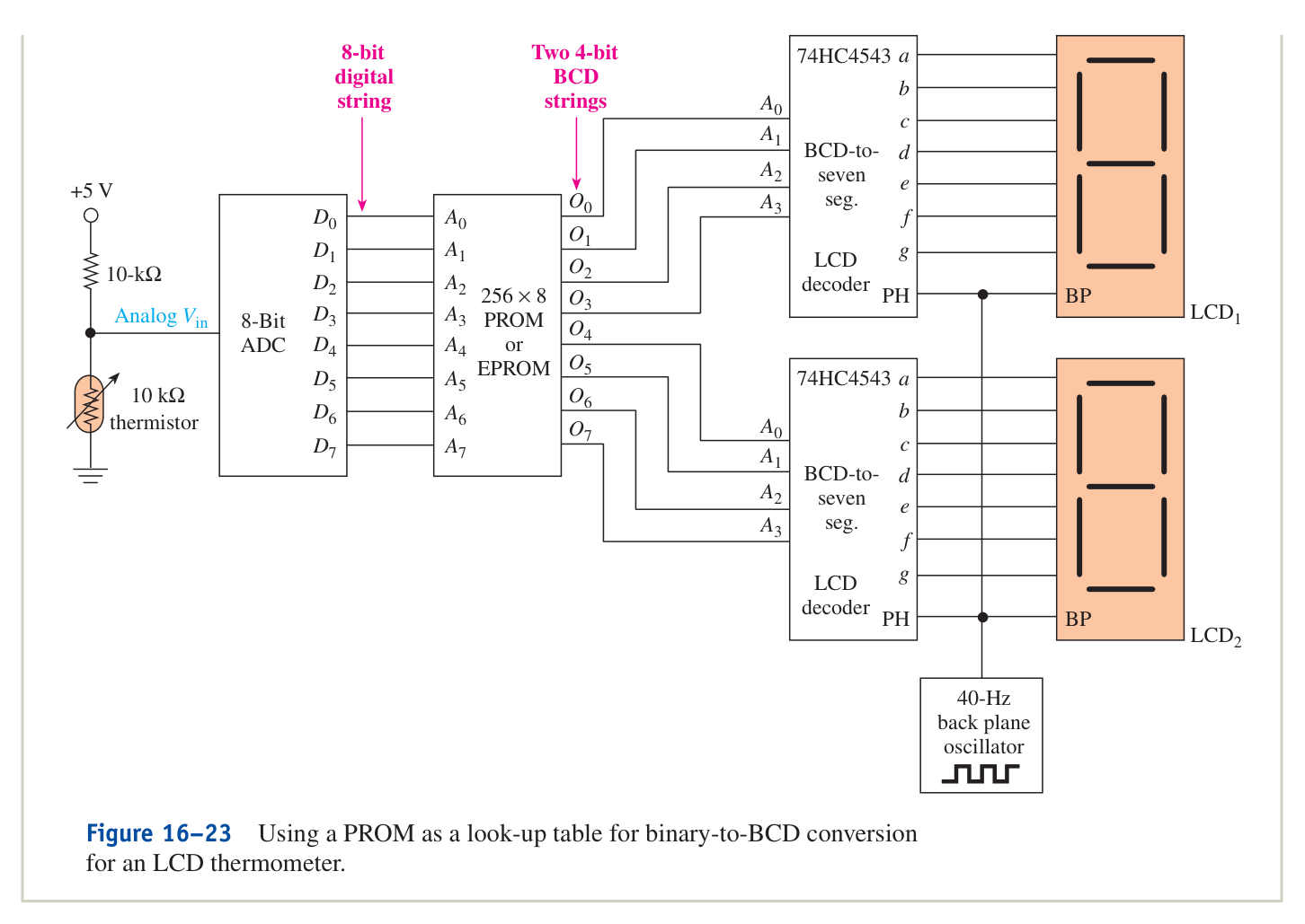
A Digital LCD Thermometer
Another application, one that covers several topics from within this text, is a digital Celsius thermometer. In this application, using a PROM look-up table simplifies the task of converting meaningless digital strings into decimal digits. Figure 16–23 shows a block diagram of a two-digit Celsius thermometer. For the circuit of Figure 16–23 to work, a binary-to-two-digit BCD look-up table has to be programmed into the PROM. Because a standard thermistor is a nonlinear device, as the temperature varies the binary output of the ADC will not change in proportional steps. Programming the PROM with the appropriate codes can compensate for that and can also ensure that the output being fed to the two decoders is in the form of two BCD codes, each within the range 0 to 9. The appropriate codes for the PROM contents
| are best determined through experimentation. For example, if at | 30�C | the |
|---|---|---|
| output of the ADC is 0100 1100 (4C16), then location | 4C16 | of the PROM |
should be programmed with 0011 0000 (30BCD). The 74HC4543 will convert its BCD input into a seven-segment code for the liquid-crystal displays (LCDs). Liquid-crystal displays consume significantly less power than LED displays but require a separate squarewave oscillator to drive their backplane. As shown in Figure 16–23, a 40-Hz oscillator is connected to the phase input (PH) of each decoder and the backplane (BP) of each LCD.
Review Questions
16–22. Determine which EPROM and which EPROM address are ac-
cessed when the microprocessor of Figure 16–20 issues a Read command for the following hexadecimal addresses: (a) READ 2002H (b) READ 0AF7H 16–23. In Figure 16–20, connect A15 to EN3 and ground EN2. What is the new range of addresses that will access the second EPROM that was formerly accessed at 1000H through 1FFFH?
| 16–24. In Figure 16–23, assume that the thermistor resistance is | 10k� | at |
|---|---|---|
| 25�C, | thus making D7 to D0 equal to 1000 0000 (one-half of full scale). |
Determine what data value should be programmed into the EPROM at address 1000 0000.
16–6 Magnetic and Optical Storage
The types of memory storage discussed so far have all been based on semiconductor material. They have relied on turning transistors ON or OFF or storing an electrical charge on a capacitor or on a floating gate of a transistor.
in nature because the memory material containing the 1s and 0s physically spins beneath a read/write head. They are nonvolatile, providing permanent storage and retrieval even when power is removed. In the case of magnetic memory, the 1 or 0 is represented on the magnetic medium as a tiny north–south or south–north polarity magnet. Optical memory differs in that it uses a laser to optically read the data stored on the medium. An indentation area (called a pit) represents 1, and a non-pit (called land) represents 0. Because of their electromechanical nature, magnetic and optical storage units are much slower and bulkier than semiconductor memory, but they are also much less expensive and provide much higher storage capacity.
Magnetic Memory: The Floppy Disk and Hard Disk
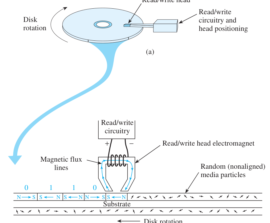
Before the advent of Flash memory, the most common removable magnetic storage for a PC was the 3.5-inch floppy disk. It consists of a magnetizable medium that spins inside a rigid plastic jacket at a speed of 300 rpm (revolutions per minute). The disk drive that holds the floppy disk (or diskette) has two read/write heads, one for each side of the diskette. They are used to record a magnetic charge to, or read a magnetic charge from, the diskette. Up to 1.44 MB of data can be stored on the double-sided diskette. The beauty of the diskette is that it can then be removed from its drive unit and used at a different location or filed away for safe-keeping. Additional diskettes can then be purchased for less than a dollar. The highest-speed magnetic storage is achieved using a hard-disk drive. This disk system is not considered a removable medium like the floppy disk, but instead, uses a series of rigid platters mounted in a sealed unit inside a PC. Its recording method is similar to the floppy, except that it uses several two-sided platters (usually three or more) to hold the magnetic data and has one read/write head for each platter surface. Because the platters are rigid and mounted in a permanent housing, their tolerances are more precisely defined, allowing for tighter spacing between bits. This also enables the disks to spin at much higher speeds (thousands of rpm). Storage capacity of hard drives is in the gigabyte range. The method of storing 1s and 0s magnetically is shown in Figure 16–24. Each disk surface is made of an iron-oxide layer capable of becoming magnetized. This sur-
face is mounted on a substrate (foundation), which is usually a flexible Mylar for the floppy disk and aluminum for the hard-drive platter. Initially, the magnetic layer consists of totally nonaligned particles representing no particular magnetic direction. By passing magnetic flux lines through the material, the particles align themselves in a specific north–south or south–north direction. As the disk surface revolves, the read/write head is moved laterally to the precise track (ring) and bit position as dictated by the PC operating system software. If the software is writing data to the disk, the control circuitry places the appropriate polarity on the electromagnet in the read/write head. The example in Figure 16–24(b) shows how to write a 1 onto the disk surface. (Four previously written bits are also shown.)
With the + to - polarity shown, magnetic flux lines will flow clockwise through the they force the particles to align in a specific direction, leaving behind a north–south
magnetic charge (south–north as you look at it.) To store a 0, the + to - polarity is remagnetic charge. To read the data, the read/write head is used as a magnetic sensor, reading the magnetic polarity as it passes beneath it. A hard drive achieves higher bit capacity and data access speed because it uses rigid disk platters revolving at a much higher speed within a precision, sealed unit. Typical rotation speed is 3600 rpm. (Some newer drives now exceed 10,000 rpm.) Because the hard drive operates in such a controlled environment, the bits can
(b)
Figure 16–24 Magnetic memory: (a) a floppy disk or hard-drive platter with one of its
read/write heads and (b) a cutaway view of Figure 16–24(a), showing how to store a south–north magnetic charge. be packed closer together. Figure 16–25 shows how the bits are laid out on a disk surface. The concentric circles on the disk are called tracks. (In the case of a hard drive, the term cylinder is used to describe the cylindrical shape that appears from the series of tracks having the same diameter on the entire stack of platters.) The Disk speed
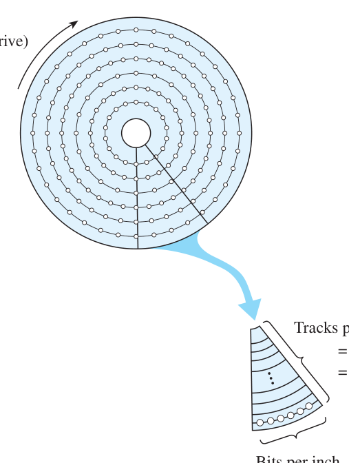
= 17,434 (floppy) = 50,000+ (hard drive)
Figure 16–25 Bit density of a floppy disk and a hard drive.
floppy diskette. Newer drives exceed 20,000 tracks per inch and 300 kilobits per inch on each track. One of the most important specifications on magnetic media is the data transfer rate. A floppy can transfer data at 45 kB/s, whereas a hard drive can exceed 30 MB/s. The slow speed of the floppy becomes annoying when you have to wait more than half a minute to transfer a large file that only takes a couple of seconds for a hard drive. Since the early 2000’s researchers have turned their attention to a new form of magnetic memory called Magnetoresistive Random Access Memory (MRAM). To date its density is not as high as a hard disk but it has many other advantages such as high speed and it has no moving parts. Address decoding is similar to a DRAM cell but instead of storing a bit as a charge on a capacitor, it stores a magnetic field on ferromagnetic plates.
Optical Memory: The CD, CD-R, CD-RW, and DVD
Music CDs have been around since the late 1970s as a digital medium for the storage and playback of analog music. In the mid-1980s, they were adopted for the storage and retrieval of digital computer data. Their data transfer rate is generally not as fast as a hard-disk drive, but manufacturers are constantly improving the speed. Because it is a removable media and capable of holding up to 650 MB of data, most new operating systems and applications software are provided on CDs.
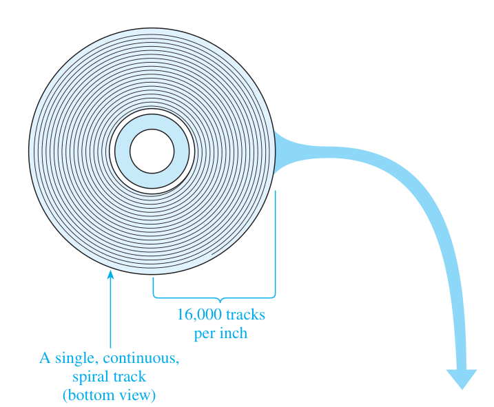
Figure 16–26 illustrates the construction of a CD. It is made of an aluminum al-
loy coating on the bottom of a rigid polycarbonate wafer. Binary data are stored on the CD by a series of indentations (called pits) representing 1s and non-pits (called lands) representing 0s. Pits are formed in the CD by stamping tiny indentations into the aluminum alloy. Data are recorded on a CD starting from the center and spiraling outward to the perimeter. The spiral is very tight, having the equivalent of 16,000 tracks per inch. A thin, plastic coating is then used to cover the CD, and a label is placed on top. As the CD spins, each bit position is read optically when a laser beam is reflected off the bottom of the CD surface. A light receptor receives the reflected light and distinguishes between light that is strongly reflected (from the land) versus light that is diffused or absent (from the pit).
Aluminum alloy 0 0 0 1 0 1 1 0 0 0 1 0 1 0 0 0 11 0 Polycarbonate wafer (substrate)
Figure 16–26 CD construction.
are manufactured with a photosensitive dye on a reflective gold layer placed on the bottom of the rigid polycarbonate wafer. To form a 1, the CD recorder superheats a tiny spot on the dye/gold layer, changing its composition so that it will not reflect the laser light in that one spot. This is not actually a pit but, instead, is just an area with reduced reflective properties. These CDs are called WORM (Write Once, Read Many) media because once they are full, they cannot be erased or rewritten. The rewritable type of CD is the CD-RW. Its surface is a silver alloy crystalline structure that is also converted into a 1 by superheating the specific bit area. The heat turns that area into its amorphous (nonreflective) state. The beauty of the CD-RW technology is that the 1 can be converted back to look like a 0 by reapplying a lowerlevel heat to that area, which returns the silver alloy back to its crystalline (reflective) state. Again, these are not actual pits and lands but, instead, are reflective and nonreflective areas. The newest standard for the CD is called DVD (Digital Versatile Disk). DVDs are not only important in the computer industry for data storage but also in home entertainment, where they are replacing prerecorded VCR tapes, offering much higher quality and greater content. They are constructed similarly to the CD but have a much higher data capacity, because the pits and tracks are packed much closer on the platter. DVDs can be single- or double-sided and have data capacities of 4.7 GB up to 17 GB.
Summary
In this chapter, we have learned the following:
- 1. A simple 16-byte memory circuit can be constructed from 16 octal D flip-
flops and a decoder. This circuit would have 16 memory locations (addresses) selectable by the decoder, with 1 byte (8 bits) of data at each location.
2. Static RAM (random-access memory) ICs are also called read/write
memory. They are used for the temporary storage of data and program instructions in microprocessor-based systems.
3. A typical RAM IC is the 2114A. It is organized as 1K * 4, which
means that it has 1K locations, with 4 bits of data at each location. (1K is actually an abbreviation for 1024.) An example of a higher-density RAM
IC is the 6206, which is organized as 32K * 8. sity than static RAMs. Their basic storage element is an internal capacitor at each memory cell. External circuitry is required to refresh the charge on all capacitors every 2 ms or less.
- 5. Dynamic RAMs generally multiplex their address bus. This means that
the high-order address bits share the same pins as the low-order address bits. They are demultiplexed by the RAS and CAS (Row Address Strobe and Column Address Strobe) control signals.
- 6. Read-only memory (ROM) is used to store data on a permanent basis. It
is nonvolatile, which means that it does not lose its memory contents when power is removed.
7. Three common ROMs are (1) the mask ROM, which is programmed
once by a masking process by the manufacturer; (2) the fusible-link programmable ROM (PROM), which is programmed once by the user; and (3) the erasable-programmable ROM (EPROM), which is programmable and UV-erasable by the user.
ing octal or hexadecimal decoders as address decoders to select the appropriate memory IC.
9. The electrically erasable PROM (EEPROM) and Flash memory use a
floating-gate MOSFET for their primary storage element. A charge on the floating gate represents the stored data.
- 10. Magnetic storage like the floppy or hard disk use magnetized particles
to represent the stored 1 or 0. Individual data bits are read and written using an electromagnetic read/write head.
- 11. Optical memory like the CD or DVD uses a laser beam to reflect light
off a rigid platter. This CD or DVD platter will have either a nonreflective pit to represent a 1 or a non-pit (land) to represent a 0.
Glossary
Address Decoding: A scheme used to locate and enable the correct IC in a system with several addressable ICs. Buffer: An IC placed between two other ICs to boost the load-handling capability of the source IC and to provide electrical isolation. Bus Contention: Bus contention arises when two or more devices are outputting to a common bus at the same time. Byte: A group of 8 bits. CAS: Column address strobe. An active-LOW signal provided when the address lines contain a valid column address. Delay Line: An integrated circuit that has a single pulse input and provides a sequence of true and complemented output pulses, with each output being delayed from the preceding one by some predetermined time period. Dynamic: A term used to describe a class of semiconductor memory that uses the charge on an internal capacitor as its basic storage element. EEPROM: Electrically erasable, programmable read-only memory. EPROM: UV-erasable, programmable read-only memory. Floating-Gate MOSFET: A special type of MOSFET, the gate of which can permanently hold an electron charge when a strong electric field is placed across it. This stored charge determines if the transistor is read as a 1 or a 0. It is the basic storage element in most EEPROM and Flash-memory ICs.
Fusible Link: Used in programmable ICs to determine the logic level at that particular location. Initially, all fuses are intact. Programming the IC either blows the fuse to change the logic state or leaves it intact. LCD: Liquid-crystal display. A multisegmented display similar to LED displays, except that it uses liquid-crystal technology instead of light-emitting diodes. Look-Up Table: A table of values that is sometimes programmed into an IC to provide a translation between two quantities. MRAM (Magnetoresistive Random Access Memory) A possible future replacement for the computer hard drive. Each memory cell consists of a magnetic charge on a stationary ferromagnetic material.
disk and hard disk used in a PC. Magnetically charged north–south particles are used to represent 1s and 0s. Individual data bits are read and written using an electromagnetic read/write head. Mask: A material covering the silicon of a masked ROM during the fabrication process. It determines the permanent logic state to be formed at each memory location. Memory Address: The location of the stored data to be accessed. Memory Cell: The smallest division of a memory circuit or IC. It contains a single bit of data (1 or 0). Memory Contents: The binary data quantity stored at a particular memory address. Optical Memory: The most common types of optical memory are the CD and DVD used by a PC. They use the reflection of a laser beam off a rigid disk platter to represent a 1 or 0. This CD or DVD platter has either a nonreflective pit to represent a 1 or a non-pit (land) to represent a 0. PROM: Programmable read-only memory. RAM: Random-access memory (read/write memory). RAS: Row address strobe. An active-LOW signal provided when the address lines contain a valid row address. ROM: Read-only memory. Semiconductor Memory: Digital ICs used for the storage of large amounts of binary
data. The binary data at each memory cell are stored as the state of a flipflop (RAM), the charge on a capacitor (DRAM), an internal transistor connection (ROM), or the charge on the gate of a floating-gate MOSFET (EEPROM, Flash). Static: A term used to describe a class of semiconductor memory that uses the state on an internal flip-flop as its basic storage element. Volatile ICs: ICs that lose their memory contents when power is removed.
Problems
Section 16–1
16–1. (a) In general, which type of memory technology is faster, bipolar or MOS? (b) Which is more dense, bipolar or MOS? 16–2. Describe the difference between the columns labeled “address” and “data” in Figure 16–1.
16–3. In Figure 16–2, all OE s are grounded. Why isn’t there a problem
| T | 16–4. Assume that the 74LS374s in the memory system in Figure 16–2 are | |
|---|---|---|
| loaded with the output of a hex counter from 00H to 0FH (H | = | Hex). |
Connecting the circuit of Figure 16–4 to Figure 16–2 allows you to test the memory system. When you read the data from the memory, you find that addresses 0000 to 0111 have the hex numbers 00H to 07H as they are supposed to, but addresses 1000 to 1111 have the same data (00H to 07H). What do you suppose is wrong, and how would you troubleshoot the system?
in Figure 16–2, using eight 74LS374s and one 74LS138.
Section 16–2
16–6. Briefly describe the difference between SRAMs and DRAMs. What
are the advantages and disadvantages of each? 16–7. Use the block diagram for the 2147H in Figure 16–5 to determine
what state CS and WE must be in to enable the three-state buffer connected
16–8. What is the level of Dout on a 2147H when CE and WE are both LOW? location within a RAM having:
(a) 1024 locations? (c) 8192 locations? 16–10. How many memory locations do the following RAM configurations have?
| (a) | 2048 * 1 | (d) | 1024 * 4 |
|---|---|---|---|
| (b) | 2K * 4 | (e) | 4K * 8 |
| (c) | 8192 * 8 | (f) | 16K * 1 |
16–11. What is the total number of bits that can be stored in the following RAM configurations?
| (a) | 1K * 8 | (c) | 8K * 8 | ||
|---|---|---|---|---|---|
| (b) | 4K * 4 | (d) | 16K * 1 | ||
| D | 16–12. Design and sketch a | 1K * 8 | RAM memory system using two | ||
| 2148Hs. (2148Hs are | 1K * 4 | with T | WE 16–13. When troubleshooting the memory system in Figure 16–7, you | and | CS.) |
keep reading incorrect values at D0 to D7. Using a logic analyzer, you observe the waveforms of Figure P16–13 at A0 to A11 and CE. What is wrong and how would you correct it?
A0–A11 New address WE = 1 25 ns 60 ns Figure P16–13
D 16–14. Use Table 16–1 to determine how many 62256 RAM ICs it would
take to design a 1MB memory system for a computer that uses 8-bit data storage.
Section 16–3
16–15. Which lines are multiplexed on DRAMs, and why?
16–16. What is the purpose of RAS and CAS on DRAMs?
(a) Draw the timing diagrams for a Read cycle and a Write cycle of a
| DRAM similar to Figure 16–11(b) and (c). Assume that | CAS | is delayed | ||||
|---|---|---|---|---|---|---|
| from | RAS | by 100 ns. Also assume that | tCAC = | 120 ns (max.), | ||
| tRAC = 180ns | (max.), | tDS = 40ns | (min.), and | tDH = | 30ns | (min.). |
| (b) How long after the falling edge of | RAS | will the data out be valid? | ||||
| (c) How soon after the falling edge of | RAS | must the data in be set up? |
16–18. How often does a 2118 DRAM have to be refreshed, and why? 16–19. What functions does the 3242 DRAM controller take care of?
Section 16–4
16–20. Are the following memory ICs volatile or nonvolatile?
| (a) Mask ROM | (c) DRAM |
|---|---|
| (b) SRAM | (d) EPROM |
16–21. Which EPROM is electrically erasable, the 2716 or the 2864?
Section 16–5
16–22. Which EPROM and which EPROM address are accessed when the
microprocessor of Figure 16–20 issues a read command for the following addresses?
| (a) READ 1020H | (c) READ 7001H |
|---|---|
| (b) READ 0ABCH | (d) READ 3FFFH? |
| D | 16–23. Redesign the connections to the 74LS138 in Figure 16–20 so that |
the four EPROMs are accessed at addresses 8000H to BFFFH.
T 16–24. When testing the EPROM memory system of Figure 16–20,
the microprocessor reads valid data from all EPROMs except EPROM2(1000H–1FFFH). What are two probable causes?
T 16–25. When the microprocessor of Figure 16–20 reads data from ad-
dresses 8000H to 8FFFH, it finds the same data as that at 0000H to 0FFFH. What is the problem?
D 16–26. In Figure 16–20, should the microprocessor software be designed
| to-HIGH edge on | RD? | Why? |
|---|---|---|
| C | D | 16–27. Design and sketch an address decoding scheme similar to Figure |
| 16–20 for an | 8K * 8 | EPROM memory system using 2716 EPROMs. (The |
| 2716 is a | 2K * 8 | EPROM.) |
16–28. What single decoder chip could be used in Figure 16–21 in place of the two 74LS138s?
| C | D | 16–29. Design a PROM IC to act like a 3-bit controlled inverter. Use a |
|---|---|---|
| 16 * 4 | PROM similar to that in Figure 16–22. When A3 is HIGH, the in- |
put at A0 to A2 is to be inverted; otherwise, it is not. Build a truth table showing the 16 possible inputs and the resultant output at Q0 to Q2 (Q3 is not used).
16–30. If at 65�C the output of the ADC in Figure 16–23 is 0111 1010
(7AH), determine what location 7AH in the EPROM should contain.
16–31. Which of the following memories are nonvolatile?
| (a) RAM | (d) Floppy disk |
|---|---|
| (b) DRAM | (e) Hard disk |
| (c) EEPROM | (f) CD |
16–32. How is a single data bit stored in the following types of memory?
(a) Magnetic memory (b) Optical memory (a) Which magnetic memory system has a higher bit density, floppy disk or hard disk? (b) Which optical memory system has a higher bit density, CD or DVD? 16–34. How does the construction of a CD-RW differ from that of a CD-R to make it rewritable?
Schematic Interpretation Problems
See Appendix G for the schematic diagrams.
S 16–35. The 62256 (U10) IC in the 4096/4196 schematic is a MOS static the size and configuration of the RAM.
S 16–36. Repeat Problem 16–35 for U6 of the HC11D0 schematic. Looking
at the connections to the address lines, determine how much of the RAM is actually accessible.
S C 16–37. The HC11D0 schematic uses two 27C64 EPROMS. (b) What are the labels of the control signals used to determine which EPROM is selected? (c) Place a jumper from pin 2 to pin 3 of jumper J1 (grid location D-6). Determine the range of addresses that make SMN_SL active (activeLOW). (d) Determine the range of addresses that make MON_SL active (activeLOW).
MultiSIM®Exercises
E16–1. Load the circuit file for Section 16–1a. The 74374 will be used as an 8-bit memory system in this circuit. The Word Generator is set up to output an 8-bit counter from 00H to FFH repeatedly. The instant that “C” is pressed, whatever is output by the Word Generator will be captured by the 8-bit D flip-flop memory system. Turn the power switch ON and press “C.” The lights that come on will be equivalent to the hex number that appeared in the Word Generator at the instant “C” was pressed. (a) Why don’t the lights change after the Word Generator continues to count up?
(b) What happens if OC is connected to VCC instead of ground? ¿
erates similar to Figure 16–20. The high-order 4 bits of the 16-bit microprocessor address bus are used to select which chip enable is activated. Determine which chip enable is activated if the microprocessor issues the following commands:
| (a) READ 2036H | (c) READ 0005H |
|---|---|
| (b) READ 4FFFH | (d) READ 8000H |
Test each of your answers.
Answers to Review Questions
16–1. Address 16–18. (a) Open source on a MOS
16–2. Data transistor. 16–3. By inputting the 4-bit address of a MOS transistor. to the 74LS154, which outputs
| a LOW pulse on one of the | (c) Having an electron charge | ||
|---|---|---|---|
| output lines when | WRITE | is | on the floating gate of a |
| pulsed LOW | MOS transistor. | ||
| 16–4. It shows when any or all of the | (d) Same as (c). | ||
| lines are allowed to change | (e) Same as (c). |
digital levels. 16–19. (a) Dissipate the electron
16–5. To avoid a bus conflict charge on the floating gate
16–6. 1024, 4 by exposing it to UV
radiation through the 16–7. LOW, HIGH open IC window. 16–8. A0 A5, A6 A11 (b) Ground the control gate
16–9. Row 7, column 9 and put a high voltage
16–10. Q5 and Q6 (VPP) on the source to
drain the electron charge 16–11. 35 ns max. off of the floating gate. 16–12. To keep the IC pin count to a (c) Same as (b). minimum. They are demulti-
| plexed by using control signals | 16–20. 120, 330 (450 total) | ||
|---|---|---|---|
| RAS | and | CAS. | 16–21. When another device has to |
use the bus 16–13. A capacitor 16–22. (a) Third EPROM, address 16–14. The charge on the internal 002H. capacitors in the RAM is
replenished. (b) First EPROM, address 16–15. 60 ms 16–23. 9000H–9FFFH 16–16. It means that when the power is
removed, the memory contents 16–24. 0010 0101 16–17. After the EPROM program has been thoroughly tested
Comments
Leave a Reply