 ChipBuddy
← Home
ChipBuddy
← Home
Why Multivoltage & Low-Power Design?
Chapter 1 — Why Multivoltage & Low-Power Design?
Power used to be an afterthought. For decades, a chip designer's mental model had exactly two knobs that mattered: make it fast (timing) and make it small (area). Power was something the package and the board engineers worried about. That world is gone. Somewhere around the 90 nm and 65 nm process generations, power quietly walked into the room and sat down at the head of the table. Today, on any serious SoC, power is a first-class constraint — designed for from the architecture down to the standard-cell pick, verified formally, and signed off with the same rigor as timing. This chapter explains why that happened and gives you a guided tour of the techniques that lowpower physical designers reach for. By the end you should be able to answer, in an interview, the deceptively simple question: "Why do we even need multivoltage design?"
The Power Problem: Two Very Different Enemies
Total power in a CMOS chip splits into two fundamentally different components, and confusing them is one of the fastest ways to look junior in an interview. Dynamic (switching) power is the energy spent charging and discharging capacitance every time a node toggles. The canonical equation is:
P_dynamic ≈ α · C · V² · f where α is the switching activity (the fraction of cycles a node actually toggles), C is the load capacitance, V is the supply voltage, and f is the clock frequency. There is also a smaller short-circuit component during the brief instant both the pull-up and pull-down networks conduct, but the CV²f term dominates the intuition. The single most important fact embedded in that formula is the V² dependency. Power scales with the square of supply voltage. Drop the voltage by 20% and you have, to first order, cut dynamic power by about 36%. That quadratic lever is the entire reason multivoltage design exists — it is simply the most powerful single knob we have for switching power. Static (leakage) power is the power a transistor burns even when it is doing nothing — sitting idle, holding a logic value. An ideal switch leaks zero current when off. Real nanometer transistors are leaky switches. The dominant contributors are subthreshold leakage (current flowing through a transistor that is nominally "off") and gate leakage (current tunneling straight through the ultra-thin gate oxide).
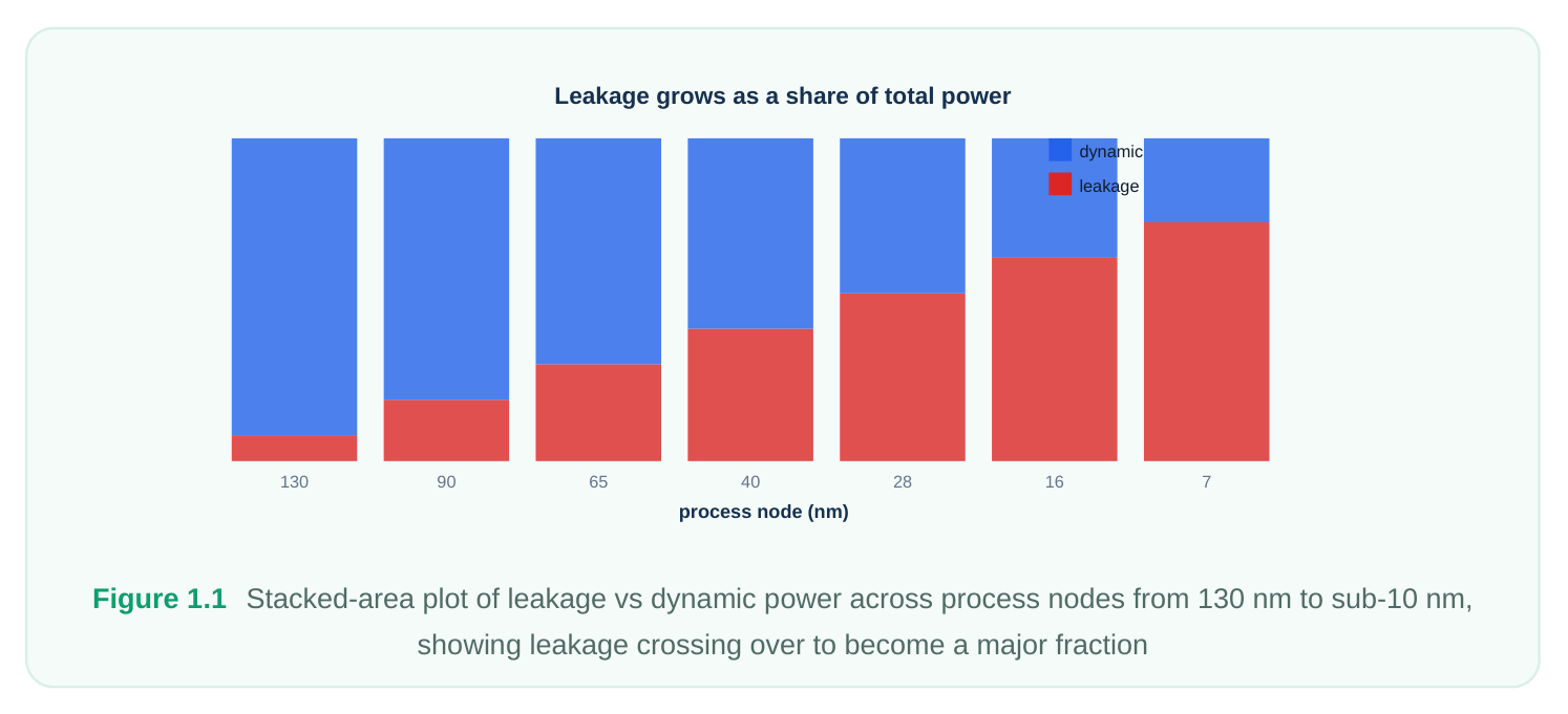
WHY LEAKAGE EXPLODED AT ADVANCED NODES
In the early days leakage was rounding error. So what changed? Three coupled trends:
- 1. Threshold voltage scaling. To keep transistors fast as supply voltage dropped, the threshold
voltage (Vt) had to drop too. But subthreshold leakage current rises exponentially as Vt falls. A modest Vt reduction can multiply leakage several-fold.
- 2. Thinner gate oxides. Shrinking oxide thickness improved control of the channel but invited
quantum-mechanical tunneling straight through the gate — gate leakage. (High-k dielectrics later pushed back on this, but the pressure never disappeared.)
- 3. Exponential transistor counts. Even if per-transistor leakage were flat, packing billions of devices
onto a die multiplies the aggregate.
The result: across several generations leakage went from a negligible sliver to, in many idle-heavy designs, a comparable share of total power — and in a phone that spends most of its life in standby, leakage can be the thing that drains the battery overnight. The crucial behavioral difference is this: dynamic power is paid only when you compute; leakage is paid as long as the block is powered, whether it works or not. That asymmetry is what motivates shutting blocks off entirely, a technique we'll meet shortly.
Power as a First-Class Constraint
Why does anyone care this much? Because power converts directly into things customers and product managers care about:
- Battery life. In mobile and wearable products, milliwatts saved translate linearly into hours of runtime. This is often the headline spec.
- Thermal limits. Every watt becomes heat. Heat must be removed, and removal costs money (heatsinks, fans) and physical space. Beyond a thermal ceiling the chip must throttle, so excess power literally caps achievable performance.
- Reliability and lifetime. Higher temperatures accelerate aging mechanisms (electromigration, bias-temperature instability). A hot chip is a chip that dies younger. Power and reliability are joined at the hip.
- Cost. Power delivery is not free: more current means more package balls, beefier on-die power grids, larger decoupling, and more expensive board regulators. A power-hungry design pays in silicon area and bill-of-materials. So when we say power is a first-class constraint, we mean it is no longer "minimize if convenient." It sits alongside timing and area as a quantity that has budgets, that gets signed off, and that can kill a tape-out if violated. The modern designer optimizes a three-way trade-off — power, performance, area (the famous PPA) — knowing that pushing any one corner tends to cost the others.
The Low-Power Toolbox at a Glance
There is no single magic technique. Real designs layer several, each attacking a different term of the power equations. Here is the working vocabulary, each with a one-line intuition and the catch.
- Multiple supply voltages (multi-VDD). Run timing-critical blocks at full voltage and relaxed blocks at a lower voltage. Intuition: exploit the V² lever block-by-block. Catch: signals crossing between voltages need level shifters, and you now manage multiple power rails.
- Clock gating. Turn off the clock to registers that aren't doing useful work this cycle. Intuition: if nothing toggles, the CV²f term goes to zero for those flops and their clock tree. Catch: requires enable logic and careful timing on the gating cell; saves dynamic power only, not leakage.
- Power gating (shutdown domains). Physically disconnect a block from its supply via header/ footer switch transistors when it is idle. Intuition: an off block leaks almost nothing — directly attacks leakage. Catch: needs isolation cells so the floating outputs don't corrupt the live logic, retention if state must survive, and a wake-up sequence that costs time and energy.
- Dynamic voltage & frequency scaling (DVFS). Adjust voltage and frequency together at run time to match the current workload. Intuition: don't pay full-speed power when half speed will do; ride the V²f curve dynamically. Catch: needs programmable regulators, characterization at multiple operating points, and software/firmware to drive it.
- Multi-Vt cell selection. The library offers cells with low, standard, and high threshold voltages. Use fast low-Vt cells only on critical paths; use leaky-stingy high-Vt cells everywhere else. Intuition: spend leakage budget only where you need the speed. Catch: low-Vt is fast but leaky, high-Vt is stingy but slow — the tool must balance them path by path.
- Body / well biasing. Apply a bias to the transistor body to dynamically nudge its threshold voltage up (reverse body bias, less leakage) or down (forward body bias, more speed). Intuition: a tunable Vt knob after fabrication. Catch: needs dedicated bias generators and bias rails; its effectiveness has weakened at the most advanced nodes.
- Operand isolation (data gating). Block the inputs of an arithmetic unit from toggling when its result won't be used. Intuition: stop a multiplier from churning on data nobody will read. Catch: adds gating logic on the datapath inputs and only helps when there is genuine wasted activity to suppress.
COMPARISON OF LOW-POWER TECHNIQUES
| Technique | Mechanism | Power saved | Primary cost / risk |
|---|---|---|---|
| Multi-VDD | Lower V on non-critical blocks | Dynamic (large) (V² lever) | Level shifters; multiple rails; floorplan complexity |
| Clock gating | Stop clock to idle registers | Dynamic | Enable logic; timing on gating cell; |
no leakage benefit
Power gating Switch off supply to idle blocks Leakage (large) Isolation + retention cells; wake-up
| DVFS | Scale V and f to workload at | Dynamic + | Programmable regulators; multi- |
|---|---|---|---|
| run time | leakage | corner sign-off; SW control | |
| Multi-Vt cells | High-Vt where slack allows, | Leakage low-Vt on critical paths | Speed/leakage trade-off; library characterization |
| Body biasing | Bias body to shift Vt up/down | Leakage (and speed tuning) | Bias rails/generators; weaker at advanced nodes |
| Operand | Gate datapath inputs when isolation | Dynamic unused | Extra gating logic; only helps with wasted activity |
A useful mental sorting: techniques in the dynamic column attack CV²f (gating, multi-VDD, DVFS, operand isolation), while techniques in the leakage column attack the always-on drain (power gating, multi-Vt, body bias). DVFS straddles both. Knowing which enemy a technique fights is exactly the discrimination interviewers probe for.
Multivoltage Means Domains That Must Coexist Safely
Here is the conceptual heart of this book. The moment you decide that different parts of the chip run at different voltages — or that some parts can be switched off entirely — you have partitioned the die into power domains: regions of logic that share a common supply, a common voltage, and a common on/ off behavior.
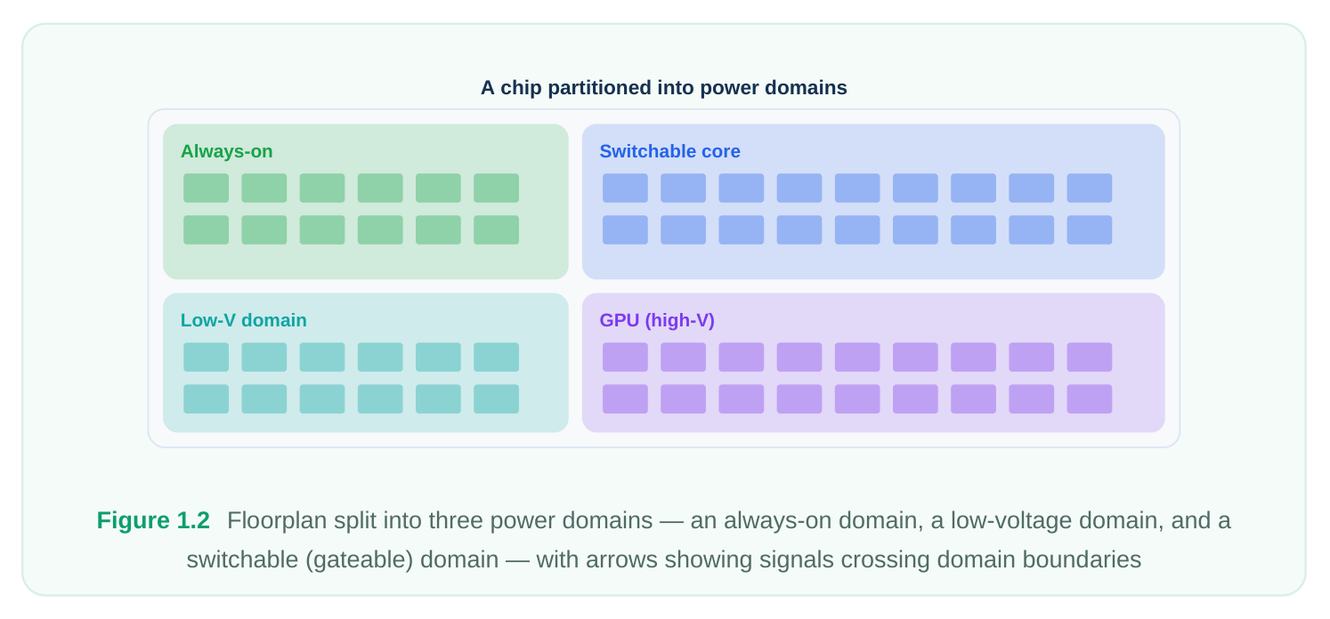
Domains are wonderful for power but they create a new class of problem at their boundaries. A signal leaving one domain and entering another no longer travels through a benign, uniform sea of logic. Consider what can go wrong:
- A signal driven at a low voltage entering a high-voltage domain may not swing high enough to be reliably recognized as a logic 1, and can leave the receiving gate's transistors partially on — wasting power and corrupting the value.
- A signal coming out of a domain that has been switched off is electrically floating. Fed into a live domain, that indeterminate value can propagate garbage, or worse, create a low-resistance crowbar path that burns power.
- When a switched-off block wakes up, any state it held has been lost. If that state mattered — a configuration register, a program counter — the system breaks. To make domains coexist safely, multivoltage design introduces special boundary cells. You will spend whole chapters on these, so for now just register their names and jobs:
- Level shifters translate a signal from one voltage to another so it is cleanly recognized on the receiving side. They are the passport control between voltage territories.
- Isolation cells clamp the outputs of a domain that is being switched off to a known, safe value (a steady 0 or 1) so downstream live logic never sees a floating input.
- Retention cells are special registers that preserve their stored value on a small always-on supply while the main supply is gated, so the block can resume where it left off after wake-up.
The pattern to internalize: multivoltage = multiple domains; multiple domains = boundary hazards; boundary hazards = special cells with explicit insertion rules. Almost everything downstream in a lowpower flow exists to place, connect, sequence, and verify those special cells correctly.
Where Low-Power Intent Enters the Flow — and Why It Must Be Formal
So how does the implementation tool know there are domains, where the boundaries are, which signals need a level shifter, where isolation clamps to, and what the power-up/power-down order is? None of this is visible in the logical RTL. A multiplier doesn't say "I live in a domain that gets switched off." The functional description is deliberately power-agnostic. This is the gap that power intent fills. The industry captures low-power architecture in a dedicated, machine-readable description — the power-intent (UPF / IEEE 1801) format, an open IEEE standard. It is a separate file that rides alongside the RTL and constraints, and it formally declares:
- the power domains and which design elements belong to each,
- the supply nets and ports and the rails that feed each domain,
- the power switches that gate the switchable domains,
- the isolation, level-shifter, and retention strategies — where these cells go and how they behave,
- and the power states — which combinations of domains-on/off-and-at-what-voltage are legal, and the sequencing between them. A minimal sketch of declaring a domain and a switch in the power-intent format looks like this:
# Declare a power domain for a switchable blockcreate_power_domain PD_CORE -elements {u_core}# Define the supply nets feeding itcreate_supply_net VDD_CORE -domain PD_COREcreate_supply_net VSS -domain PD_CORE -reuse# Insert a power switch so the domain can be shut downcreate_power_switch sw_core \-domain PD_CORE \-output_supply_port {vout VDD_CORE} \-input_supply_port {vin VDD} \-control_port {sleep pwr_ctrl/sleep_en} \-on_state {ON vin {!sleep}}And declaring the boundary protection — isolation on the way out, retention for the state:
# Clamp PD_CORE outputs to a safe value while it is powered down
set_isolation        iso_core \
-domain        PD_CORE \
-isolation_power_net VDD \
-clamp_value   0 \
-applies_to    outputs
# Preserve critical state across the power-down
set_retention        ret_core \
-domain        PD_CORE \
-retention_power_net  VDD \
-retention_ground_net VSS
Why must this be formal rather than scribbled in a spec? Three reasons:
- 1. A single source of truth. The same power-intent file drives synthesis, place-and-route, and
verification. If the intent lived only in a document, each tool would re-interpret it and the implementations would drift apart.
- 2. Automatic cell insertion. Because the intent is precise, the tool can automatically insert the right
level shifters, isolation cells, and retention flops at exactly the right boundaries — far more reliably than a human editing netlists by hand.
- 3. Formal verification. A separate checker can prove that every crossing is protected, every
shutdown domain is isolated, no retention is missing, and every power state is reachable and legal — before you commit silicon. You cannot formally verify a paragraph of English. You can formally verify a power-intent file. Realizing intent: PM-cell insertion
| Power intent | Match library | Insert & place | Tie controls & | Re-verify |
|---|---|---|---|---|
| (strategies) | PM cells | cells | supplies |
Figure 1.3 Flow showing RTL + power-intent file feeding synthesis, then place-and-route, with a parallel formal
low-power verification step checking the intent at each stage The payoff of capturing intent early and formally is that low-power decisions become consistent and checkable across the whole flow, instead of a pile of fragile manual edits that one mistake can turn into a dead chip.
Interview Q&A
cost? Dynamic power follows α·C·V²·f, so it scales with the square of voltage. A 20% voltage reduction cuts dynamic power by roughly a third. The cost is that lower voltage slows transistors, so
you can only do it on blocks with timing slack — and any signal crossing from a low-voltage to a higher-voltage domain needs a level shifter to be read correctly.
statement? Power gating targets leakage, not dynamic power. Switching a block's supply off removes the always-on static current it would otherwise burn while idle. Dynamic power is only consumed when nodes toggle; to attack that you'd use clock gating, multi-VDD, operand isolation, or DVFS. The confusion conflates the two distinct power components.
negligible? Three coupled effects: thresholds dropped (to preserve speed at lower supply voltage), and subthreshold leakage rises exponentially as Vt falls; gate oxides thinned, inviting tunneling current; and transistor counts exploded, multiplying any per-device leakage. Unlike dynamic power, leakage is paid whenever a block is powered, idle or not — which is why always-on, mostly-idle products feel it most.
file? The RTL is intentionally power-agnostic — it describes function, not which logic shares a rail or gets switched off. A formal power-intent file (UPF / IEEE 1801) provides one machine-readable source of truth that drives synthesis, implementation, and verification identically, lets the tool auto-insert isolation, level-shifter, and retention cells at the right boundaries, and lets a formal checker prove every crossing is protected before tape-out. None of that is possible with prose.
Key Takeaways
- Total power splits into dynamic (α·C·V²·f, paid only when computing) and static/leakage (paid whenever powered, idle or not); these are different enemies needing different weapons.
- Leakage exploded at advanced nodes due to lower thresholds, thinner oxides, and exploding transistor counts — making "just turn it off" (power gating) a real strategy.
- Power is now a first-class constraint alongside timing and area, driven by battery life, thermal limits, reliability, and cost — the PPA trade-off.
- The toolbox layers many techniques; sort them by whether they fight dynamic power (clock gating, multi-VDD, DVFS, operand isolation) or leakage (power gating, multi-Vt, body bias).
- Multivoltage = multiple power domains that must coexist safely, which creates boundary hazards and the need for level shifters, isolation cells, and retention cells.
- Low-power architecture is captured formally and early in the power-intent (UPF / IEEE 1801) format, giving a single source of truth that enables automatic cell insertion and formal verification before silicon.
Comments
Leave a Reply