 ChipBuddy
← Home
ChipBuddy
← Home
Library Requirements for Low-Power Design
Chapter 3 — Library Requirements for Low-Power Design
A multivoltage, power-gated chip is only as trustworthy as the cell library underneath it. Ordinary logic libraries assume a single power rail, a single ground, and a world in which every gate is always alive. Multivoltage design breaks all three assumptions: voltages differ between blocks, supplies switch on and off, and some logic must survive while everything around it goes dark. To make that work, the library must ship a catalog of special cells and, just as importantly, must describe those cells precisely enough that automated tools can recognize, place, and verify them without a human pointing at each one. This chapter walks through that catalog, the multi-rail modeling that backs it, the multi-Vt and corner story, the attributes that let tools self-select cells, and the failure modes when the library is incomplete. A useful mental model: power intent (expressed in an open standard such as IEEE 1801) declares what the design wants — these domains, these supplies, these isolation rules. The library declares what is physically available to satisfy that intent. When the two disagree — intent asks for a cell type the library never characterized — the flow either errors out or, worse, silently substitutes something wrong.
Why ordinary cells are not enough
Consider two adjacent voltage domains. A net leaving a 0.72 V domain and entering a 1.0 V domain carries a signal whose "high" is well below the receiver's switching threshold scaled to its rail. The receiving gate may interpret it as a weak, slow, or crowbar-inducing input — burning DC current as both transistors of an input inverter partially conduct. No ordinary buffer fixes this; you need a cell that translates voltage levels. Likewise, when a domain is switched off, its outputs float. A floating input into a live domain is electrically undefined and can again drive crowbar current. Ordinary logic has no concept of "my neighbor just powered down." These structural problems are why the special-cell catalog exists.
The special-cell catalog
The table below summarizes the family; the subsections expand on each.
| Cell type | Primary purpose | Typical location | Key pins beyond logic I/O |
|---|---|---|---|
| Level shifter | Translate signal swing between rails | Domain-to-domain crossings | Input-side and output-side power pins |
| Isolation cell | Clamp a powered-down | Output boundary of a output to a safe value | Isolation enable; both rails switchable domain |
| Retention flop | Preserve state through power-down | Inside switchable domains | Save/restore controls; retention (always-on) supply |
| Power-switch | Connect/disconnect a | Distributed across the | Enable in/out; true and virtual |
| (header/footer) | domain's virtual supply | switched domain | supply pins |
| Always-on buffer/ | Drive control nets that must cell | Routed through dark live during sleep | Always-on backup supply pin regions |
| Power-gating | Sequence switch enable/ controller | In always-on region acknowledge | Sleep request, acknowledge, daisy-chain |
| Tie cell (for gated | Provide stable logic-0/1 | Inside switchable domains) | Domain-aware power pin domains |
LEVEL SHIFTERS (UP, DOWN, DUAL-RAIL)
A level shifter converts a logic swing referenced to one rail into a swing referenced to another. An up- shifter takes a low-voltage signal into a higher-voltage domain; this is the harder direction, because a weak low input must reliably flip a high-rail stage, so the cell uses a cross-coupled (often half-latch) topology. A down-shifter is simpler and sometimes a plain buffer suffices, but a characterized downshifter guarantees timing and avoids current spikes. A dual-rail level shifter physically exposes both power pins — the input-side rail and the output-side rail — so the cell can be characterized and connected to each independently. Some level shifters also embed isolation (an enable that holds the output during shutdown), giving an "enable level shifter" that does two jobs at one boundary. Key pins: the data in/out plus two power connections. Tools must know which power pin belongs to the source domain and which to the destination — that mapping is part of the library description, not something inferred from placement.
ISOLATION CELLS (CLAMP-HIGH, CLAMP-LOW, LATCH)
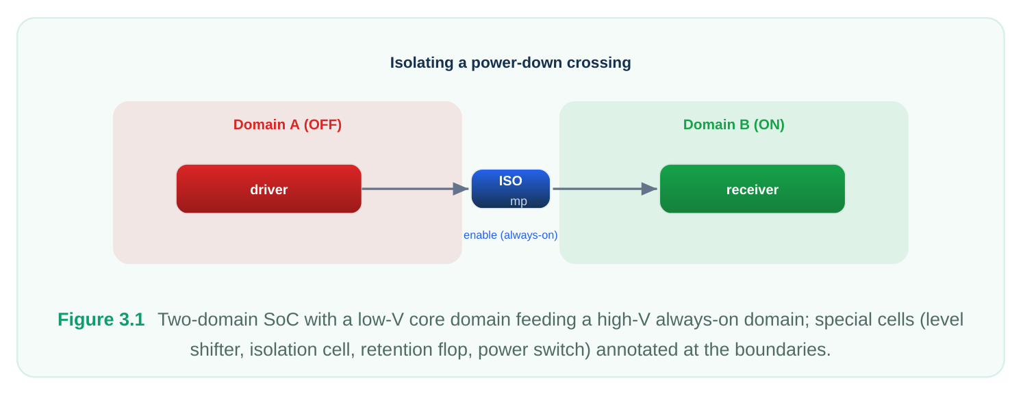
An isolation cell sits on a net that leaves a domain which may power down, and it forces a known value when the source is off. A clamp-low cell (typically an AND-style structure with an active-low enable) drives 0; a clamp-high (OR-style) drives 1; a latch-type isolation cell holds the last valid value. The choice is dictated by what the receiving logic needs to see during sleep — for example, an activelow reset line usually wants clamp-high so it stays inactive. The isolation enable comes from alwayson control logic, and the cell itself must be powered from a supply that stays up while the source domain is down. A subtle but vital requirement: the isolation enable must assert before the source
supply collapses and de-assert after it is restored — sequencing that the power-management controller and the verification flow must both honor.
RETENTION FLOPS (SAVE/RESTORE)
A retention flop keeps its state while its main domain is powered off. Internally it has a normal masterslave path on the switchable supply plus a small balloon latch on an always-on retention supply. A save event copies the live value into the balloon before shutdown; a restore event copies it back after power returns. The cost is a second power pin (the retention supply, which must remain live during sleep) and the save/restore control pins, plus modest area and leakage overhead in the always-on portion. Because only the balloon stays alive, a retention flop holds state at a fraction of the always-on cost of leaving the whole flop powered.
POWER-SWITCH CELLS (HEADER / FOOTER)
These are the transistors that gate a domain's supply. A header switch (PMOS) sits between true VDD and the domain's virtual VDD; a footer switch (NMOS) sits between domain ground and true ground. The switch has an enable input and usually an enable output so many switches can be chained, charging the domain gradually to limit inrush (rush-current) and ground bounce. Switches come in coarse-grain (a ring or column structure feeding a whole block) and fine-grain (per-cell) flavors. The library must model the on-resistance and the true-versus-virtual supply pins so IR-drop and timing tools see the real picture.
ALWAYS-ON BUFFERS AND CELLS
Some nets — isolation enables, switch enables, retention controls, sleep handshakes — must remain valid while the region they pass through is dark. An always-on cell carries a backup supply pin so it stays powered even when the local domain's primary supply is gated. Physically these cells may sit inside a switched region but be tied to the always-on rail, letting control signals route through "dark" silicon safely.
POWER-GATING CONTROL CELLS
The handshake that turns a domain off and on — request, acknowledge, switch-chain sequencing, isolation/retention ordering — is implemented by control cells living in the always-on region. They ensure the legal order: assert isolation, save retention, open switches; and on wake, close switches, wait for the supply to settle, restore, then release isolation.
TIE CELLS FOR GATED DOMAINS
A constant logic-0 or logic-1 must come from a tie cell rather than a hard rail tap, for reliability. In a switchable domain, the tie cell must be powered from the domain's supply (so the constant tracks the domain's power state) or, when the constant must persist, from an always-on supply. The library distinguishes these, and the flow must pick the variant matching the net's domain.
Multi-rail / multi-voltage characterization
Every special cell above shares one demand: it touches more than one supply. An ordinary library view models a single VDD/VSS pair and bakes the supply into the timing implicitly. A multivoltage library must expose explicit power and ground (PG) pins and characterize behavior as a function of each relevant supply. This is "secondary-PG" modeling: the timing/power view declares a primary supply and one or more secondary supplies (the input-side rail of a level shifter, the retention rail of a flop, the true-supply side of a switch) and states how the cell behaves across their states.
| Primary supply | Secondary supply (must be | ||
|---|---|---|---|
| Cell | Behavior tied to secondary | ||
| (modeled) | modeled) | ||
| Up-level | Output-domain rail | Input-domain rail | Input thresholds, valid |
| shifter | translation | ||
| Retention flop | Switchable domain rail | Retention rail | State held when primary is |
off
| Isolation cell | Always-on/destination | Source domain rail | Clamp value when source |
|---|---|---|---|
| rail | off | ||
| Header | Virtual VDD (domain | True VDD switch | On-resistance, voltage drop side) |
If the secondary rail is not declared in the library view, downstream tools assume the cell uses only the primary supply. They will then connect it to a single rail, mis-time it, and pass verification that should have failed — a classic source of silent bugs.
Multi-Vt families and PVT corners
Independent of multivoltage, leakage is managed through multi-Vt (multi-threshold) cell families. The same logic function ships in several flavors:
| Family | Threshold | Speed | Leakage | Where used |
|---|---|---|---|---|
| HVT (high-Vt) | High | Slow | Lowest | Non-critical paths, leakage-sensitive |
blocks
SVT/RVT (standard/ Medium Medium Medium General-purpose default
LVT (low-Vt) Low Fast Highest Timing-critical paths only SVT/HVT on paths with slack. Effective use needs all families characterized at consistent footprints so swaps are drop-in.
Multivoltage operation multiplies the corner problem. A cell that runs at several voltages must be characterized at each operating voltage across process and temperature — a grid of PVT (process, voltage, temperature) corners. A block that operates at 0.72 V in a low-power mode and 1.0 V in a turbo mode needs library data at both, at slow/typical/fast process and across the temperature range, plus the special temperature-inversion corner where low-voltage logic is fastest cold or hot depending on the node. Missing a voltage point forces risky interpolation or blocks that operating mode entirely.
How the library advertises each cell's role
Automated insertion only works if a tool can look at a cell and know what it is for. Libraries therefore carry function attributes that label each special cell — flags marking a cell as a level shifter (with its direction and the rails it bridges), as an isolation cell (with clamp polarity and enable sense), as a retention flop (with save/restore pin roles), as a switch (with enable-in/enable-out and the supply it gates), or as always-on. These attributes, combined with the PG-pin declarations, let the implementation flow query "give me an up-shifter from domain A's rail to domain B's rail with isolation" and get the right cell automatically. The power-intent file references cell types or named strategies; the matching is resolved against these attributes. A simplified power-intent sketch (open-standard style) that relies on those attributes:
# Define the supplies and a switchable power domain
create_supply_port  VDD_HIGH
create_supply_port  VDD_LOW
create_power_domain  PD_CORE -elements {u_core}
# Insert isolation on outputs of the switchable core,
# clamping low; tool selects a cell flagged as isolation
set_isolation iso_core \
-domain        PD_CORE \
-isolation_power_net VDD_HIGH \
-clamp_value   0 \
-applies_to    outputs
# Insert level shifters where PD_CORE drives the high domain
set_level_shifter ls_core \
-domain     PD_CORE \
-applies_to outputs \
-rule       low_to_high
And a sketch of how a retention strategy points at the always-on retention supply and the save/restore controls:
# Keep core state across power-down using retention flops
set_retention ret_core \
-domain               PD_CORE \
-retention_power_net  VDD_HIGH \
-save_signal   {save_n  negedge} \
-restore_signal {save_n posedge}
# Map the abstract supplies onto real states/voltages
add_power_state VDD_LOW  -state {ON  -voltage 0.72}
add_power_state VDD_LOW  -state {OFF -voltage 0.0}
In both cases the tool does not invent circuitry — it picks library cells whose attributes match the requested role and wires their special pins to the named supplies and control signals.
What goes wrong with incomplete library support
Library gaps are among the most painful multivoltage bugs because they often pass early checks and surface late.
- Missing secondary-PG modeling. If a retention flop's retention rail or a level shifter's input rail is absent from the library view, connectivity tools wire only the primary supply. Power-aware verification then sees a "normal" cell and reports no violation, while silicon either loses state on power-down or fails to translate levels — a functional failure with no warning in the reports.
- Uncharacterized level shifters. A level shifter present in layout but lacking proper multi-rail timing/ power data gets timed against a single supply. Setup/hold numbers are wrong, the path may be unconstrained, and the crowbar-current risk the shifter was meant to remove is invisible to power analysis.
- Missing function attributes. Without the role flags, the tool cannot auto-select cells; engineers fall back to manual instantiation, which scales badly and invites human error (wrong clamp polarity, wrong direction shifter).
- Incomplete corner coverage. A voltage operating point with no characterized data forces interpolation or simply forbids that low-power mode, defeating the design's power strategy.
- Inconsistent multi-Vt footprints. If HVT/SVT/LVT variants differ in pin placement or size, leakage- recovery swaps are no longer drop-in and the optimizer cannot trade speed for leakage freely. The common thread: the physical cell may exist, but if the library does not describe its extra rails, control pins, and role, the tools treat it like ordinary logic and the design's power intent is quietly violated.
Interview Q&A
how does that affect characterization? An up-shifter must let a weak low-voltage input reliably switch a higher-rail output stage, so it uses a cross-coupled/latch topology that pulls the output to the high rail rather than passing the input through. A down-shift can often be a buffer because the input
swing already exceeds the lower-rail thresholds. For characterization, the up-shifter's behavior depends explicitly on both the input-side and output-side supplies, so its library view must declare two PG pins and be characterized across both voltages; a down-shifter still benefits from dual-rail modeling but is electrically more forgiving.
a library view of supplies beyond the primary one — the retention rail of a flop, the input rail of a level shifter, the true supply of a switch — along with how the cell behaves as those rails change state. Without it, connectivity and verification tools assume a single supply, connect only that rail, time the cell incorrectly, and pass power-aware checks that should fail. The result is silent loss of retention, broken level translation, or missed crowbar current.
attributes in the library plus PG-pin declarations. Each cell is flagged with its role (level shifter and direction, isolation with clamp polarity, retention with save/restore roles, switch with enable-in/out, always-on). The power-intent file requests a strategy ("isolate these outputs, clamp 0," "low-to-high shift here," "retain state on this domain"), and the flow resolves that request against the attributes to choose a matching cell and connect its special pins.
designs? Because each operating voltage is effectively a new electrical condition. A cell used at 0.72 V and 1.0 V must be characterized at both, and at low voltages the process/temperature sensitivity is sharper, including temperature-inversion effects. Multiply operating voltages by process and temperature corners and the corner count grows quickly. Missing a corner forces interpolation (inaccurate) or removes that low-power operating mode from the design.
Key Takeaways
- Multivoltage design requires a catalog of special cells — level shifters, isolation cells, retention flops, power switches, always-on cells, power-gating control, and domain-aware tie cells — none of which exist in ordinary single-rail libraries.
- Every special cell touches more than one supply, so the library must model secondary-PG pins and characterize behavior across each rail's states.
- Multi-Vt families trade speed for leakage; consistent footprints across HVT/SVT/LVT make leakage-recovery swaps drop-in.
- Multivoltage operation demands a dense PVT corner grid, one set per operating voltage.
- Function attributes let tools auto-select the right cell from power intent; without them, insertion becomes manual and error-prone.
- Incomplete library support — missing secondary-PG data, uncharacterized shifters, absent role flags — produces silent failures that pass early checks and surface in silicon. The physical cell existing is not enough; the library must fully describe it.
Comments
Leave a Reply