 ChipBuddy
← Home
ChipBuddy
← Home
Well / Body Biasing
Of all the knobs available to a low-power designer, body biasing is the most quietly powerful and the most frequently misunderstood. It does not gate a supply, it does not stop a clock, and it does not insert a single buffer into your datapath. Instead it reaches underneath the transistors and adjusts the very voltage at which they decide to turn on. Mastering this technique means understanding a little device physics, a few practical supply-network realities, and a handful of power-intent declarations that interviewers love to probe. This chapter walks through all three.
The Physics: Why the Body Terminal Matters
A MOSFET is a four-terminal device, even though schematics usually draw only three. The fourth terminal is the body (also called the bulk or well). For an NMOS device the body is the p-well; for a PMOS device it is the n-well. In a standard cell, the p-well is normally tied to ground and the n-well is normally tied to the supply, so we lazily forget the body exists. Body biasing is simply the act of deliberately driving those well terminals to a voltage other than the rails. Why does that help? Because the threshold voltage, Vt, is not a fixed constant. It depends on the voltage between the source and the body, through the body effect: Vt = Vt0 + γ · ( √(2φ_F + V_SB) − √(2φ_F) )
The exact form is less important than the intuition. The body terminal modulates the depletion charge under the channel, and that charge sets how hard you must push the gate to form a channel. Move the body voltage, and you move Vt. There are two directions you can push:
- Reverse Body Bias (RBB): make the body voltage less favorable than the source. For NMOS, drive the p-well below ground (negative); for PMOS, drive the n-well above the supply. This raises Vt. A higher Vt means dramatically less subthreshold leakage (leakage falls roughly exponentially with Vt) but slower switching, because the gate overdrive shrinks.
- Forward Body Bias (FBB): make the body voltage more favorable than the source. For NMOS, drive the p-well slightly positive; for PMOS, drive the n-well slightly below the supply. This lowers Vt, boosting speed at the cost of much higher leakage and a small risk of forward-biasing the source-body junction if you overdo it.
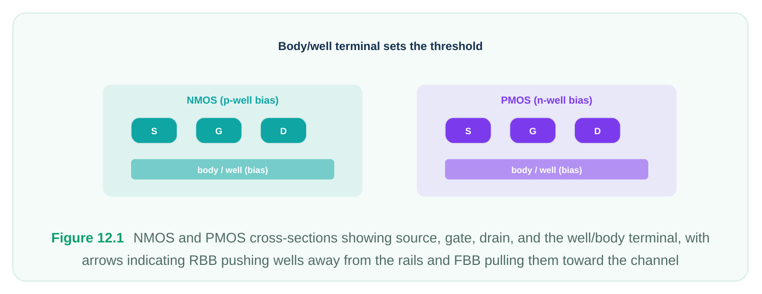
The reason this is such an attractive low-power knob is that it is continuous, reversible, and applied post-fabrication. Unlike multi-Vt selection — which is baked into the mask and cannot change after tape-out — body bias can be dialed at runtime. You can leak less when the chip is idle, run faster when the workload spikes, and compensate for a slow corner of silicon by leaning on FBB. It is the closest thing the physical designer has to a tuning dial on finished hardware.
Static, Adaptive, and Per-Domain Biasing
Body biasing strategies fall along a spectrum of sophistication. Static body bias applies a single fixed bias level chosen at design time. The most common use is a permanent RBB applied to blocks that are usually idle (large caches, deeply pipelined accelerators that sit dormant), trading a little speed for a large standby-leakage win. It is cheap: one extra bias rail, one fixed generator, no control logic. Adaptive body bias (ABB) closes a control loop. On-chip sensors — ring-oscillator speed monitors, leakage monitors, or temperature sensors — feed a controller that adjusts the bias level dynamically.
ABB is the technique that turns body bias from a static trade-off into a genuine optimizer. Its two flagship use cases are:
- 1. Process compensation. A slow die gets FBB to claw back lost speed; a fast, leaky die gets RBB
to suppress excess leakage. This tightens the distribution and improves yield.
- 2. Workload and thermal tracking. Bias follows demand — FBB during bursts, RBB during idle —
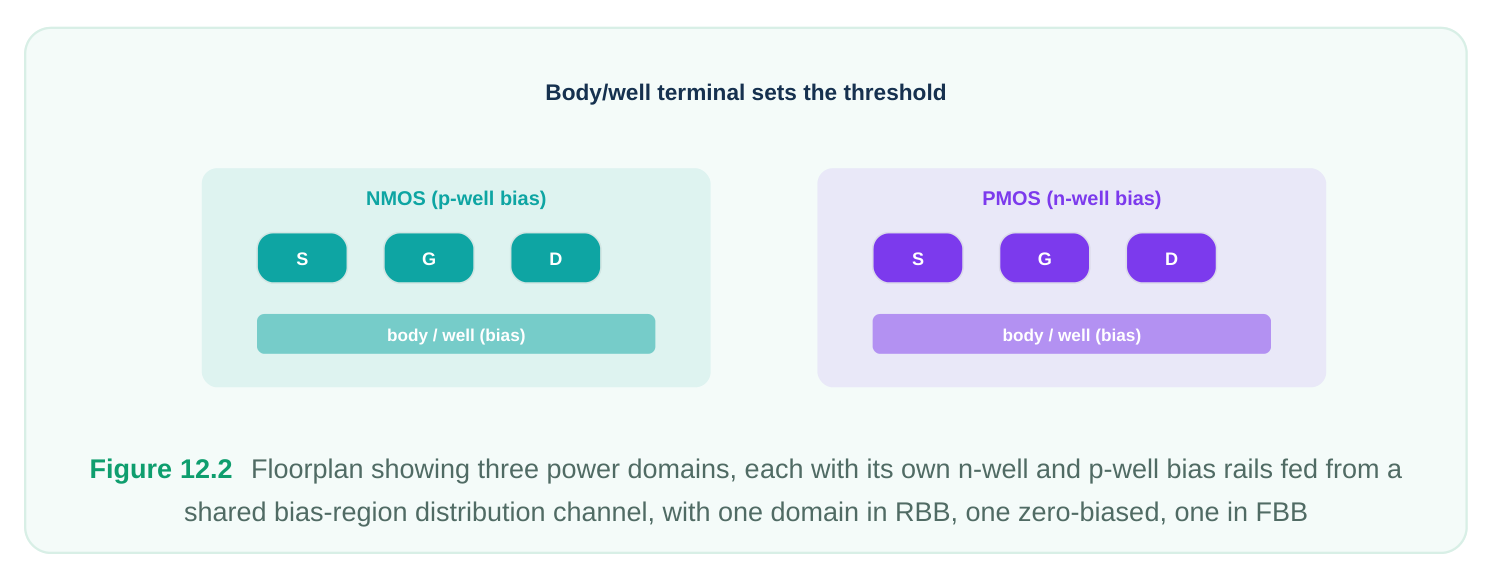
and backs off when the part runs hot. Per-domain bias recognizes that one bias level rarely suits the whole chip. A high-performance core and a low-leakage I/O block want opposite treatment. So the die is partitioned, and each power domain gets its own bias rails and its own generator, allowing independent tuning.
Bias Supplies and Bias Networks
Body bias introduces voltages that simply do not exist in a conventional design: a p-well rail that may sit below ground, and an n-well rail that may sit above the supply. These cannot share routing with the ordinary power grid. The physical implications are real:
- Two extra bias rails per biased domain. Conventionally named in generic terms as the p-well bias (often VBBN / negative-going for NMOS wells) and the n-well bias (often VBBP / above-rail for PMOS wells). These are low-current rails — bias supplies source almost no DC current because they drive reverse-biased junctions — so they can be thin, but they must be continuous across the well region.
- A bias region or bias channel. The wells of all cells in a domain must connect to the bias rails. This is done through dedicated well-tap cells that contact the well and tie it to the bias rail rather than to the conventional rail. The taps must be placed densely enough to keep well resistance low; sparse taps leave the interior of the well floating at a different potential than the rail, undermining the bias.
- A bias generator. The negative and above-rail voltages are produced on-chip by charge pumps or regulators, packaged as bias generator cells. In an adaptive scheme the generator is programmable and sits inside the control loop.
A common interview trap: candidates assume bias rails carry significant current and over-design the network. They do not. The subtlety is reliability and uniformity, not current — keep the well potential flat across the domain and respect the negative/above-rail levels in your electromigration and IR signoff setup.
Declaring Bias in Power Intent
This is where the open power-intent standard (IEEE 1801) enters. In a non-biased design, a supply set has two functions: power and ground. A bias-enabled supply set adds two more functions — the nwell bias and the p-well bias — so that every cell in the domain knows which net drives its wells. The conceptual flow is: create the bias nets, build a supply set that includes the extra well-bias functions, and associate that supply set with the domain.
# Create the well-bias supply nets alongside the conventional rails
create_supply_net VDD       -domain CORE
create_supply_net VSS       -domain CORE
create_supply_net VNW_BIAS  -domain CORE   ;# n-well bias (PMOS bodies)
create_supply_net VPW_BIAS  -domain CORE   ;# p-well bias (NMOS bodies)
# A bias-enabled supply set carries four functions, not two
create_supply_set CORE_SS \
-function {power  VDD} \
-function {ground VSS} \
-function {nwell  VNW_BIAS} \
-function {pwell  VPW_BIAS}
The presence of the nwell and pwell (well-bias) functions is exactly what marks the supply set — and therefore the domain — as bias-enabled. Tools use this to demand bias-aware cells, to insert the correct taps, and to run the bias-specific connectivity checks. You then attach the supply set to the power domain and state the legal bias voltages as part of the operating modes, so timing and leakage are evaluated at the right body-bias points:
# Associate the bias-enabled supply set with the domain
set_domain_supply_set CORE_DOMAIN -supply_set CORE_SS
# Define the bias states the domain is allowed to use
add_power_state CORE_SS \
-state {RBB_MODE  -supply_expr {power == 0.80 && nwell == 1.05 && pwell ==
-0.25}} \
-state {ZERO_BIAS -supply_expr {power == 0.80 && nwell == 0.80 && pwell ==
0.00}} \
-state {FBB_MODE  -supply_expr {power == 0.80 && nwell == 0.55 && pwell ==
0.20}}
Notice how each state pins the well-bias functions to specific values. In RBB the n-well sits above the supply (1.05 V vs 0.80 V rail) and the p-well sits below ground (−0.25 V) — both wells pushed away
from the channel. In FBB the wells move toward the channel. The zero-bias state ties the wells to the rails and behaves like a conventional design. Defining these states is what lets verification confirm that the body bias your library was characterized at actually matches the bias your power intent intends.
Coexisting Bias and Non-Bias Blocks
Real SoCs are heterogeneous. A leakage-critical compute domain might be bias-enabled while a small always-on controller is conventional. The standard supports this: only the supply sets that declare wellbias functions are biased; the rest carry the usual two functions. The boundary discipline is what matters. The hard rule — and a favorite interview question — is that you cannot drop a non-bias-aware cell into a bias-enabled domain. A conventional cell ties its wells internally to its power and ground pins. If you place it in a region where the bias rails are at −0.25 V and 1.05 V, the cell's wells never see the bias; worse, its internal tie can short the intended bias rail to a conventional rail through the well, defeating the bias and creating a reliability hazard. The cell was also never characterized at the bias point, so its timing is simply wrong. The mirror-image mistake is also common: declaring a bias-enabled supply set but forgetting to define one of the well-bias supplies, leaving (say) the p-well bias net unconnected. The wells then float, the bias does nothing, and silicon behaves unpredictably.
Library and Physical Prerequisites
Body biasing is not free at the library level. You need:
- Bias-aware standard cells whose well-tie pins are brought out to the bias rails rather than hard- tied internally, so the placement-and-route engine can connect them to the bias network.
- Well-tap cells specific to the biased domain, distributing the bias potential across the wells.
- Characterization at the bias points. Each cell must be re-characterized (timing, leakage, and noise) at every bias level you plan to operate in. A cell library characterized only at zero bias gives you no trustworthy numbers for RBB or FBB modes. This is often the gating cost of adopting body bias — the silicon supports it, but the library investment is what stops teams. Requirement Conventional design Bias-enabled design Supply-set functions power, ground power, ground, n-well bias, p-well bias Well taps tie wells to rails tie wells to dedicated bias rails Cell well pins hard-tied internally brought out to bias rails Library characterization nominal rails per-bias-point (RBB / zero / FBB) Extra routing none two low-current bias rails + bias channel On-chip generators none charge pumps / regulators (+ controller if adaptive)
Pitfalls, Checks, and When to Skip Them
The verification step that catches body-bias errors is a dedicated bias connectivity / bias consistency check. It confirms that every bias-enabled domain has all four supply functions defined and connected, that all cells in the domain are bias-aware, that well taps reach the bias rails, and that the bias voltages in the power states are ones the library was actually characterized at.
| Pitfall | How it shows up | Resolution |
|---|---|---|
| Non-bias cell in a bias | Bias check flags an unbiased/ | Swap to the bias-aware equivalent; |
| domain | internally-tied well; timing mismatch | restrict the library set for the domain |
| Missing a well-bias | Floating well net; bias check error | Create the missing bias net and add it to |
| supply | on undefined function | the supply set |
| Sparse well taps | Non-uniform well potential; IR/ | Increase tap density in the bias region |
reliability warnings
| Bias state not in | No valid timing/leakage at that bias | Add the corner or restrict states to |
|---|---|---|
| characterization set | point | characterized points |
| Forward-biasing | Excess junction leakage, latch-up junctions in FBB | Cap FBB magnitude to a safe device limit risk |
When is it legitimate to skip the bias checks? Only when there is genuinely no bias in the design — every supply set carries just power and ground and no cell exposes well pins. Running bias checks on a purely conventional design wastes runtime and can produce noise. But the moment a single domain becomes bias-enabled, those checks are mandatory and should never be waived; the failure modes they catch are silent in functional simulation and only surface as leakage or speed surprises in silicon.
Worked Conceptual Example
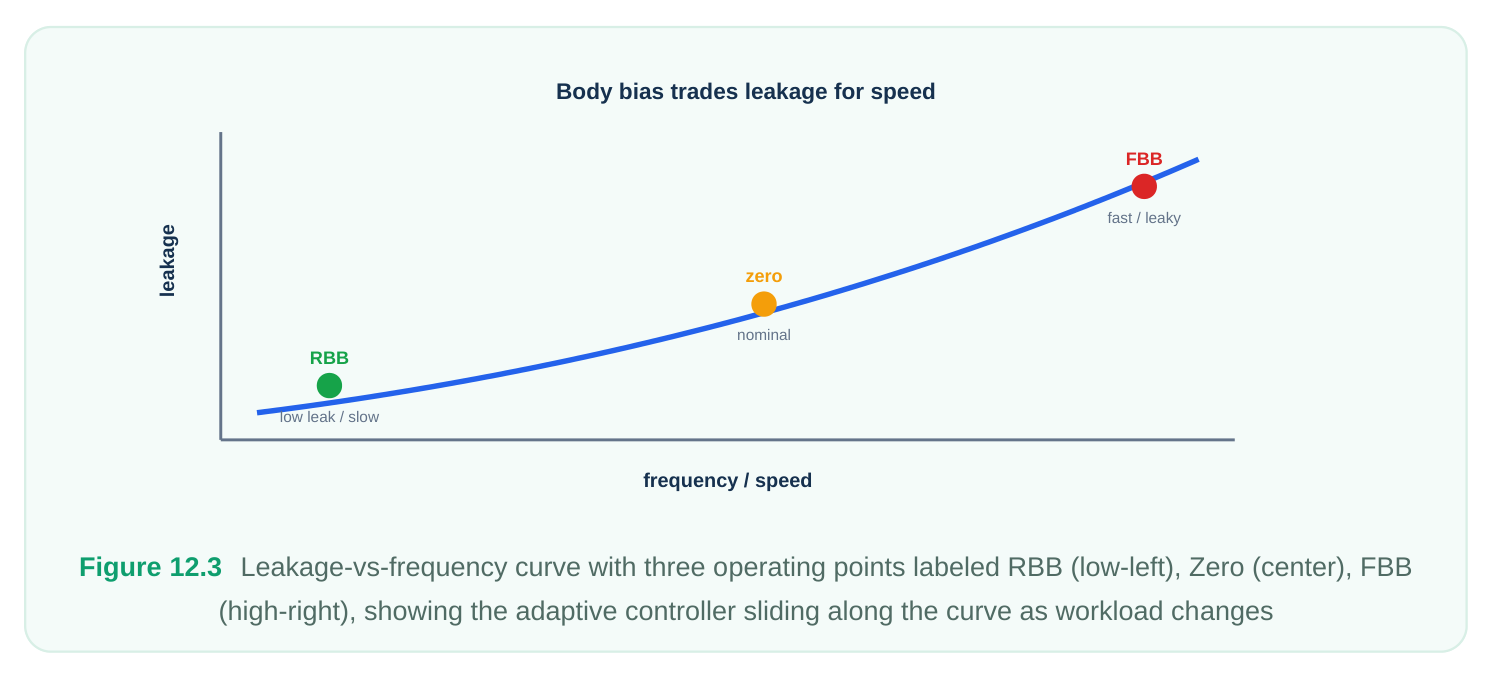
Consider an SoC with a compute cluster that bursts hard but idles most of the time, and a sensor-hub that runs continuously at low speed. You make the compute cluster a bias-enabled domain with an adaptive controller, and you leave the sensor-hub conventional. During idle, the controller drives the compute cluster into RBB: the n-well goes above the rail, the pwell below ground, Vt rises, and standby leakage drops by a large factor — exactly what you want when the cluster contributes nothing but heat. When a workload arrives, the speed monitor reports a slow path and the controller swings to FBB, lowering Vt and recovering the frequency headroom needed to hit the deadline, accepting the leakage penalty only for the duration of the burst. Between the two, zero bias is the neutral resting state. The sensor-hub, untouched by all of this, keeps its wells on the conventional rails and never participates in the bias network. The qualitative trade-offs across the three modes:
Bias
Well direction Vt Leakage Speed Typical use
| RBB | wells pushed away | higher | much | slower | idle / standby leakage reduction |
|---|---|---|---|---|---|
| from channel | lower | ||||
| Zero | wells on the rails | nominal | nominal | nominal | conventional / neutral operation |
bias
| FBB | wells pulled toward | lower | much | faster | performance bursts / slow-die |
|---|---|---|---|---|---|
| channel | higher | speed recovery |
Interview Q&A
terminal away from the channel, increasing the depletion charge the gate must overcome, which raises Vt. Subthreshold leakage falls roughly exponentially with Vt, so even a few hundred millivolts of RBB yields a large leakage reduction. The cost is speed: a higher Vt shrinks the gate overdrive, so paths run slower. It is ideal for idle blocks where the speed loss does not matter.
conventional supply set declares only power and ground. A bias-enabled supply set adds two more functions — the n-well bias and the p-well bias. Their presence tells the tools to require bias-aware cells, insert taps that route to the bias rails, and run bias connectivity checks. It also lets you pin specific well voltages in each power state so the design is verified at the same bias points the library was characterized at.
caught? The conventional cell ties its wells internally to its power/ground pins instead of to the bias rails. The wells never receive the intended bias, the cell's timing — characterized only at zero bias — is wrong, and the internal tie can short a bias rail to a conventional rail through the well, a reliability
hazard. The bias connectivity check catches it by flagging the internally-tied or unbiased well. The fix is to swap in the bias-aware equivalent and restrict the domain's library to bias-aware cells.
and is cheapest — good for permanently-idle blocks needing leakage reduction. Adaptive bias closes a loop with on-chip monitors and is preferable when conditions vary: compensating process spread (FBB for slow dies, RBB for leaky ones), tracking workload (FBB for bursts, RBB for idle), and backing off under thermal stress. ABB costs sensors, a controller, and a programmable generator, but it converts a static trade-off into a runtime optimizer.
Key Takeaways
- The body terminal modulates Vt through the body effect; RBB raises Vt (less leakage, slower), FBB lowers Vt (faster, more leakage).
- Body bias is uniquely valuable because it is continuous, reversible, and applied post-silicon — the designer's one true runtime tuning dial.
- Bias-enabled domains need two extra low-current rails (n-well and p-well bias), well taps that reach them, on-chip generators, and a bias channel; current is small but well-potential uniformity is critical.
- In power intent, a bias-enabled supply set carries four functions (power, ground, n-well bias, p-well bias); define each bias mode as a power state pinning the well voltages to characterized points.
- Bias and non-bias domains can coexist, but never place a non-bias-aware cell in a bias domain, and never leave a well-bias supply undefined.
- Library cost is the real gate: cells must expose well pins and be characterized at every bias point you intend to operate.
- Always run bias connectivity/consistency checks on any bias-enabled design; only skip them when no bias exists at all.
Comments
Leave a Reply