 ChipBuddy
← Home
ChipBuddy
← Home
Power Gating with Power Switches
Of all the levers a low-power designer can pull, power gating delivers the single largest leakage win. Voltage scaling slows leakage; multi-threshold cell swaps trim it; clock gating kills dynamic activity. But none of them reach the floor that power gating reaches, because power gating does something fundamentally different: it physically disconnects an idle block from its supply rail. When the supply is gone, there is essentially nothing left to leak. This chapter explains how that disconnect is built, controlled, and sequenced, and why getting the sequence wrong is one of the most expensive mistakes in a low-power flow.
Why Cut the Supply at All
Leakage current flows whenever a transistor is powered, even when nothing is switching. In advanced nodes, leakage can account for a large fraction of total power, and for a block that spends most of its life idle — a co-processor, an audio engine, a rarely used accelerator — that idle leakage is pure waste. Clock gating stops the dynamic component but leaves the standby leakage untouched. Power gating attacks the standby leakage head-on by inserting a switch transistor in series between the always-on supply and the gated block. Open the switch and the block floats; its leakage drops by orders of magnitude. This technique is often called MTCMOS, for multi-threshold CMOS. The name comes from the standard practice of building the gated logic from low-threshold (fast, leaky) transistors while building the switch itself from a high-threshold (slow, low-leakage) device. The high-threshold switch leaks very
little when off, so it does not undo the savings, yet it can still pass enough current to power the block when on. The result is a region that runs fast when awake and leaks almost nothing when asleep. It helps to frame power gating against the other low-power techniques rather than in isolation. Clock gating eliminates the dynamic power of an idle block but leaves every transistor powered and therefore still leaking. Operand isolation and data gating stop unnecessary toggling deeper in the datapath, again addressing dynamic power only. Voltage scaling and body biasing reduce leakage but cannot eliminate it, because the transistors remain connected to a supply. Power gating is categorically different: by removing the supply, it drives leakage toward the residual level of the offstate switch itself, which is typically two to three orders of magnitude below the powered leakage of the block. That is why power gating is reserved for blocks with meaningful idle time — the entry and exit overhead only pays back if the block stays off long enough, a break-even point sometimes called the minimum sleep time.
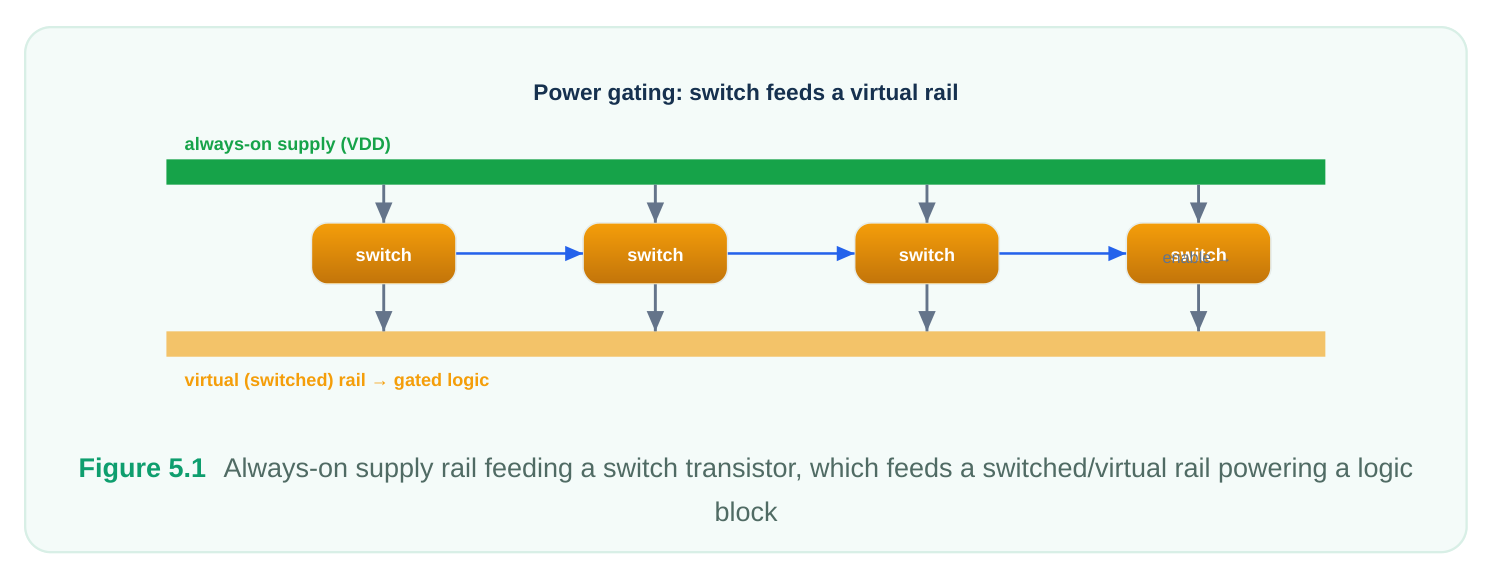
The price of this win is never free. The switch adds series resistance, consumes area, requires its own control network, and — most subtly — demands careful sequencing with the isolation and retention mechanisms covered in earlier chapters. The rest of this chapter walks through each of these costs and how to manage them.
Header Switches vs Footer Switches
The switch can be placed on either end of the supply path. A header switch is a PMOS device inserted between the true supply (VDD) and the block's local supply rail. A footer switch is an NMOS device inserted between the block's local ground rail and the true ground (VSS). Either one breaks the current path and shuts the block down; the choice between them is a trade-off.
| Aspect | Header (PMOS to VDD) | Footer (NMOS to GND) |
|---|---|---|
| Device type | PMOS | NMOS |
| What it gates | The supply rail | The ground rail |
| Area for equal drive | Larger (lower hole mobility) | Smaller (higher electron mobility) |
| Protects against | Supply-side leakage | Ground-side leakage |
| Virtual rail created | Virtual VDD | Virtual VSS (virtual ground) |
| Noise sensitivity | Sees supply noise | Footer bounce couples into ground |
NMOS footers are smaller for a given on-resistance because electrons are more mobile than holes, so they need less width to pass the same current. That makes footers area-efficient. However, gating the ground rail creates a "virtual ground" that floats above true ground when the switch is partially on, and any disturbance there couples directly into the block's ground reference, which can be hazardous for sensitive analog-adjacent logic. PMOS headers are larger but keep the ground reference clean, and many designers prefer them when the gated block must coexist with always-on neighbors that share the same ground. Some designs even use both for maximum isolation, at the cost of double the switch overhead. In practice, header switches are the more common choice in digital low-power SoCs, largely because a solid, shared ground is easier to reason about during signoff.
Switch Granularity: Fine-Grained vs Coarse-Grained
Once you have chosen header or footer, the next decision is how the switches are distributed. Fine-grained power gating embeds a switch transistor inside each standard cell, or in a small cluster of cells. Every gated cell carries its own switch. This gives excellent local control and predictable percell behavior, but it is expensive: the switch overhead is paid on every single cell, the library must contain switched variants of everything, and the area penalty is severe. Fine-grained gating is rare in mainstream digital design for these reasons, though it appears in specialized libraries. Coarse-grained power gating is what almost everyone uses. Here a fabric of switch cells — a ring around a region, columns interspersed through the placement, or a combination — feeds an entire block through a shared virtual rail. The ordinary logic cells are standard, unswitched cells; they simply connect to the virtual rail instead of the true rail. A relatively small number of switch cells, sized as a group, power the whole region.
| Property | Fine-grained | Coarse-grained |
|---|---|---|
| Switch location | Inside each cell | Shared fabric (ring/columns) |
| Library impact | Switched variant per cell | Small set of switch cells |
| Area overhead | High | Moderate, amortized |
| Control complexity | Distributed | Centralized fabric control |
| Typical usage | Specialized | Mainstream SoC blocks |
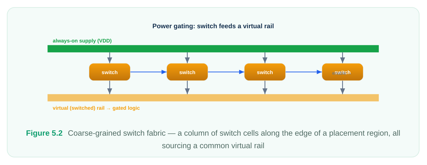
The switch cells in a coarse-grained design form a switch array. They are physically placed as part of the region, their true-rail pins tie to the always-on supply, and their switched-rail pins tie together into the virtual (switched) supply rail that the logic draws from. Sizing this array — how many switches, how wide — is a central design problem we return to below.
Controlling the Switches: Enable, Daisy-Chain, and Acknowledge
A switch network needs a control signal that tells it to turn on or off. The naive approach — drive every switch's gate from a single net at the same instant — is a recipe for disaster. When hundreds of switches turn on simultaneously, an enormous inrush current (also called rush current) flows as the discharged virtual rail charges back up to the supply voltage. That current spike drags the always-on supply down, injects noise everywhere, and can cause ground bounce severe enough to corrupt neighboring logic or even reset retention storage. The standard solution is staged, sequenced turn-on. The switch cells are wired in a daisy-chain: the enable signal enters the first switch, and each switch's enable output feeds the next switch's enable input, so the wave of turn-on propagates down the chain with a controlled delay between stages. Only a few switches turn on at any moment, the virtual rail charges gradually, and the inrush current is spread out over time into a manageable ramp rather than a violent spike.
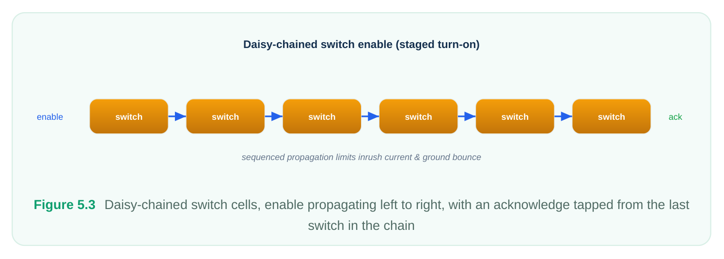
Many switch cell styles also offer two parallel chains: a small "weak" switch that turns on first to gently pre-charge the rail, followed by a "strong" switch that turns on once the rail is mostly charged to provide the full current capacity. This two-step ramp limits inrush even further. The far end of the daisy-chain produces an acknowledge signal. Because the enable had to propagate through every switch to reach the end, seeing the acknowledge assert tells the controller that the entire chain is on and the rail is (nominally) fully powered. The power management controller waits for this acknowledge before it allows the block to be used again. The acknowledge is the handshake that makes power-up safe: never assume the rail is ready; wait for the chain to confirm it.
Sequencing: The Order That Must Not Be Violated
Power gating does not live alone. It interacts tightly with isolation cells (which clamp a powered-down block's outputs to a safe constant value) and retention registers (which preserve critical state across the off period). The order in which these mechanisms engage is not a stylistic preference — it is a correctness requirement. Powering down, the order is: isolate, then save, then power down.
- 1. Isolate the block's outputs first, so that as the supply collapses the floating, indeterminate outputs
are clamped to safe values and cannot propagate garbage into always-on logic downstream.
- 2. Save retained state into the retention cells (assert the save/restore control so the balloon latches
capture the live values) while the block is still powered.
- 3. Power down by de-asserting the switch enable. The virtual rail collapses; leakage drops to near
zero. Powering up, the order reverses: power up, then restore, then de-isolate.
- 1. Power up by asserting the switch enable and waiting for the acknowledge — the rail must be fully
restored before any logic is trusted.
- 2. Restore retained state from the retention cells back into the now-powered registers.
- 3. De-isolate last, releasing the output clamps only after the block is powered and its state is valid, so
the outputs it presents to the rest of the chip are correct from the first cycle.
Power-down / power-up sequencing clock gate isolation save (retention) power switch order: gate →isolate →save →switch off (reverse to wake)
Figure 5.4 Two timelines — power-down (isolate, save, switch off) and power-up (switch on, ack, restore, de-
isolate) Violate this order and the failures are silent and intermittent: de-isolate too early and garbage escapes; restore before the rail is up and the restore fails; skip isolation and a collapsing block injects glitches into a neighbor. These bugs are notoriously hard to find in simulation and brutal to debug in silicon, which is why the sequence is encoded explicitly in the power intent and verified.
Sizing the Switch Network
The switch array must be wide enough to deliver the block's peak current without dropping too much voltage across itself, yet narrow enough to keep area and off-state leakage in check. This is the core sizing tension. When the block is active, current flows from the true rail through the switch on-resistance to the virtual rail. That on-resistance causes an IR drop: the virtual rail sits slightly below the true rail. If the drop is too large, the gated logic effectively runs at a reduced voltage, slowing it down and possibly violating timing. To reduce IR drop you add more switches in parallel (lowering total resistance) or use wider switches. But every switch you add costs area and, even as a high-threshold device, leaks a little when off — so an oversized switch network erodes the very leakage savings power gating exists to deliver. The art is to size for the worst-case active current at an acceptable IR drop, then stop. A useful rule of thumb is to budget a small percentage of the supply voltage as the maximum tolerable IR drop across the switches, compute the required total on-conductance from the block's peak current, and divide by the per-switch conductance to get the switch count — then add margin for placement reality and process variation. The peak current of interest is the active worst case, not the inrush, because inrush is controlled separately by sequencing. One detail that trips up newcomers: the control network must be always-on. The enable, the daisychain wiring, the acknowledge, and the buffers driving them cannot themselves be powered by the rail they are switching — that would be circular. They must be routed on the always-on supply and built from always-on cells. Forgetting this means the very logic meant to wake the block has no power to do
so. There is also a placement and physical dimension to sizing that signoff cannot ignore. The switch cells are not lumped in one spot; they are distributed across the region so that the virtual rail is charged
uniformly and no corner of the block is starved. A switch array clustered at one edge would leave the far cells seeing a larger effective resistance and a deeper IR drop, creating a timing gradient across the block. Distributing the switches as columns or a ring also spreads the inrush current spatially, which eases the burden on any single segment of the always-on power grid. Finally, the always-on grid that feeds the switches must itself be robust enough to source the inrush ramp without sagging, so power-grid analysis of the gated region is done with the switches modeled explicitly rather than as ideal connections.
Worked Conceptual Example
Below is a conceptual sketch of how a coarse-grained header switch network is expressed in standard power-intent commands. Names are illustrative. First, define the switch for a gated power domain, specifying the output (switched) supply, the input (always-on) supply, and the control logic that maps the enable to the switch's on/off state.
# Define a header power switch for the gated domain
create_power_switch sw_audio \
-domain        PD_AUDIO \
-output_supply_port {vout VDD_AUDIO_SW} \
-input_supply_port  {vin  VDD_ALWAYS_ON} \
-control_port  {sleep_in  pg_enable} \
-ack_port      {sleep_out pg_ack} \
-on_state      {on_state vin {!sleep_in}}
Next, the logical switch is bound to a physical switch cell from the library — the cell that actually carries the high-threshold transistor and the daisy-chain ports. This mapping step is where the abstract intent meets a real library cell.
# Map the logical switch onto a physical switch-cell type
map_power_switch sw_audio \
-lib_cells     {HEADER_SW_HVT} \
-port_map      {{vin VDDG} {vout VVDD} \
{sleep_in NSLEEPIN} {sleep_out NSLEEPOUT}}
Finally, sketch the controller handshake in behavioral pseudo-form: assert the enable, wait for the acknowledge, and only then proceed. This is the safety interlock that prevents using a block before its rail is up.
# Power-up handshake (conceptual controller behavior)
set pg_enable 1                ;# request power-up, kicks off daisy-chain
wait_until {pg_ack == 1}       ;# block until chain fully on, rail restored
restore_retention PD_AUDIO     ;# pull saved state back into registers
set iso_enable 0              ;# de-isolate last: outputs now valid
The corresponding full switching sequence, in both directions, is summarized below.
| Step | Power-Down Sequence | Power-Up Sequence |
|---|---|---|
| 1 | Quiesce clocks to the domain | Assert switch enable (start daisy-chain) |
| 2 | Assert isolation (clamp outputs) | Wait for acknowledge (rail confirmed up) |
| 3 | Assert save (capture retention state) | Stabilize / settle delay |
| 4 | De-assert switch enable (rail collapses) | Assert restore (reload retention state) |
| 5 | Domain now in low-leakage off state | De-assert isolation (release outputs) |
| 6 | — | Release clocks; domain fully active |
Reading the two columns together makes the symmetry clear: isolation brackets the powered-off interval on both ends, retention save pairs with retention restore, and the switch enable is the innermost action on power-down but, paired with its acknowledge, the outermost gate on power-up.
Interview Q&A
while the gated logic uses low-Vt cells? The switch spends most of its life off, so its off-state leakage directly subtracts from the savings power gating is meant to deliver; a high-Vt device leaks very little when off. The logic inside the block, by contrast, needs to be fast when awake, so it benefits from low-Vt cells. Combining a high-Vt switch with low-Vt logic is the essence of MTCMOS: low leakage at the gate, high performance inside.
When a gated block powers up, its collapsed virtual rail must recharge to the supply voltage, and if all switches turn on at once an enormous current spike flows to charge that rail. This spike can crash the always-on supply and cause ground bounce that corrupts neighboring logic. A daisy-chain wires the switch enables in series so turn-on propagates as a controlled wave, charging the rail gradually and spreading the current over time. Two-stage weak-then-strong switches limit it further by pre-charging gently before the full current capacity engages.
matters. Power-down is isolate, save, power down. Isolation must come first so the collapsing block's indeterminate outputs are clamped before they can propagate garbage; save must happen while the block is still powered so retention cells capture valid state; then the supply is cut. Power-up reverses it: power up and wait for acknowledge, restore, then de-isolate. The rail must be confirmed up before any logic is trusted, state must be restored before the block operates, and isolation is released last so the outputs presented to the rest of the chip are valid from the first cycle. Wrong order produces silent, intermittent corruption.
Size it for the block's worst-case active current at an acceptable IR drop across the switch onresistance — typically a small percentage of the supply. More or wider switches lower IR drop but cost area and add a little off-state leakage, so you size for the worst case and stop, adding margin for variation. The acknowledge, tapped from the end of the daisy-chain, confirms that the enable has propagated through every switch and the rail is fully powered; the controller must wait for it before using the block. Note the control network itself must be always-on, since it cannot be powered by the rail it switches.
Key Takeaways
- Power gating delivers the largest leakage reduction available by physically disconnecting an idle block's supply; MTCMOS pairs a high-Vt switch with low-Vt logic to keep both leakage low and performance high.
- Header switches (PMOS, gate VDD) keep the ground clean but are larger; footer switches (NMOS, gate GND) are smaller but expose the block to virtual-ground noise.
- Coarse-grained gating with a shared switch fabric feeding a virtual rail is the mainstream choice; fine-grained per-cell gating is rare due to area cost.
- Daisy-chained enables with staged turn-on limit inrush current and ground bounce; the acknowledge at the chain's end is the handshake confirming the rail is up.
- Sequencing is a correctness requirement: isolate, save, power down on the way out; power up, restore, de-isolate on the way back.
- Size the switch array to meet worst-case active current within an IR-drop budget, balancing it against area and off leakage, and always route the control on an always-on supply.
Comments
Leave a Reply