 ChipBuddy
← Home
ChipBuddy
← Home
Logical Effort & Gate Sizing
Sizing Gates the Smart Way
Every gate can be made bigger or smaller. Bigger gates drive loads faster. But they also load the gate before them. So you cannot just make everything huge. There is a best size for each stage. "Logical effort" is a simple method to find it. It turns sizing from guesswork into a quick calculation. This chapter explains it in plain terms, with worked numbers.
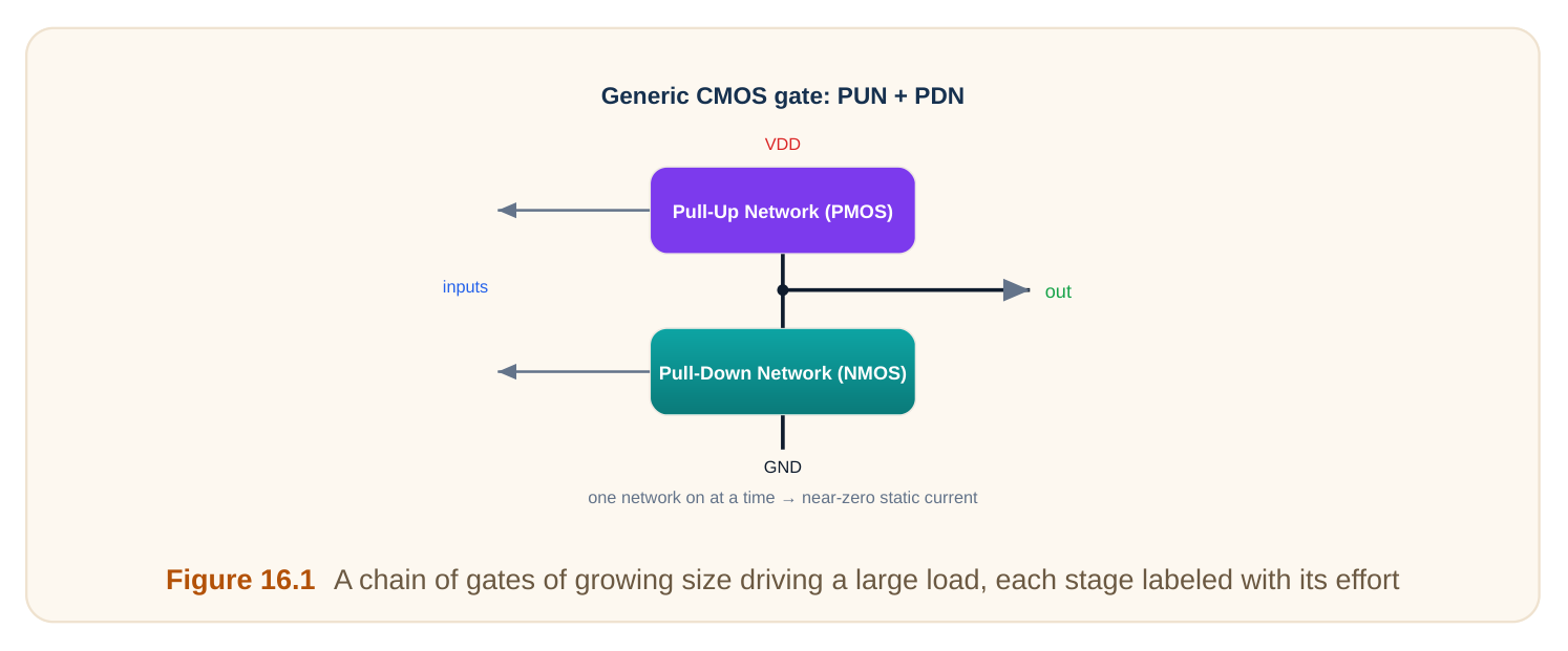
The Three Pieces of Delay
A gate's delay has three plain parts.
- Logical effort (g): how much harder a gate is to drive than a simple inverter. An inverter has g = 1. A NAND is a bit worse. A NOR is worse still.
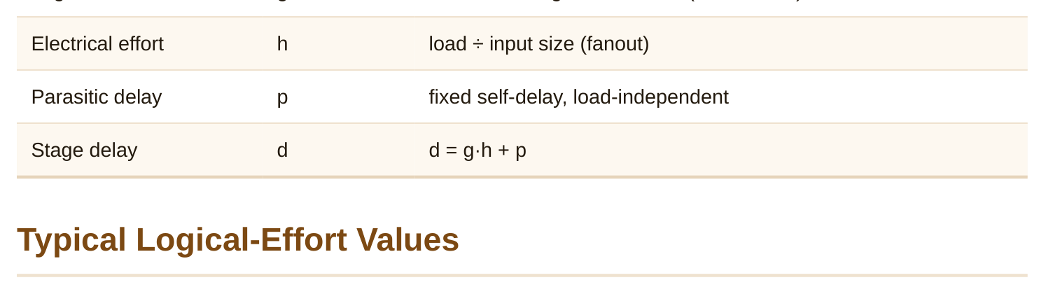
- Electrical effort (h): the load it drives divided by its own input size. This is just "fanout" in size terms.
- Parasitic delay (p): a fixed delay from the gate's own internal capacitance. It does not depend on the load. The delay of one stage is: d = g × h + p. The g×h part is the "effort delay". The p part is the fixed cost. This little formula is the whole tool. Term Symbol Plain meaning Logical effort g how hard the gate is to drive (inverter = 1)
Different gate types have different g. The reason: series transistors must be made wider to keep the same drive, which raises input capacitance. More inputs in series means higher g.
| Gate | Logical effort g (rough) | Parasitic p (rough) |
|---|---|---|
| Inverter | 1 | 1 |
| 2-input NAND | 4/3 | 2 |
| 2-input NOR | 5/3 | 2 |
| 3-input NAND | 5/3 | 3 |
Note the NOR is worse than the NAND. That is because PMOS is weaker, and the NOR stacks PMOS
in series. So designers prefer NAND-based logic when speed matters.
Worked example — one gate's delay
A 2-input NAND (g = 4/3, p = 2) drives a load four times its input size (h = 4).
d = g·h + p = (4/3)(4) + 2 = 5.33 + 2 = 7.33 delay unitsCompare an inverter (g = 1, p = 1) driving the same h = 4:
d = (1)(4) + 1 = 5 delay unitsThe NAND is slower for the same job. That is the cost of doing real logic.
Driving a Big Load: the Path Method
The real power is sizing a chain of gates to drive a big load fast. The method has a few steps.
- 1. Path logical effort (G): multiply the g of every stage.
- 2. Path electrical effort (H): total load ÷ first input size.
- 3. Path effort (F): F = G × H × b, where b accounts for any branching.
- 4. Best stage effort: each stage should have effort f = F^(1/N), where N is the number of stages.
- 5. Best number of stages: roughly when each stage's effort is about 3 to 4.
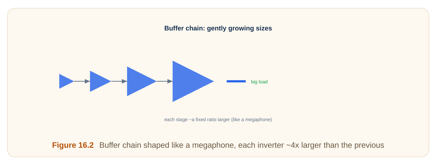
The key insight: spread the work evenly. Each stage should multiply the size by about the same factor. That factor is near 4 (often quoted as e ≈ 2.7 in theory, ~3–4 in practice).
Worked example — how many buffers?
You must drive a load 64 times the size of your first inverter. Only inverters are used, so G = 1. Branching b = 1. So path effort F = 1 × 64 × 1 = 64. Try different stage counts. The best stage effort is F^(1/N).
| Stages N | Stage effort F^(1/N) | Comment |
|---|---|---|
| 1 | 64 | one giant gate — far too slow |
| 2 | 8 | better |
| 3 | 4 | near ideal (~4) |
| 4 | 2.83 | also good |
Three stages give a per-stage effort of 4. That is right in the sweet spot. So use about three inverters, each ~4× the last. The sizes grow 1 → 4 → 16 → 64.
Worked example — total path delay
For the 3-stage solution above, each stage has effort delay 4. Add the parasitic (p = 1 per inverter):
total delay = N × (stage effort + p) = 3 × (4 + 1) = 15 delay unitsA single giant inverter would be 64 + 1 = 65 units. So staging is more than 4× faster. That is the whole point.
Why Effort Near 4 Is Best
Too few stages: each stage has a huge electrical effort, so it is slow. Too many stages: you pay too many fixed parasitic delays. The best point balances these. Math puts the ideal stage effort near e (≈ 2.7), but parasitics push the practical value to about 3–4. So "fan out by about 4 per stage" is the rule of thumb.
| Choice | Effect |
|---|---|
| Too few stages | each stage overloaded → slow |
| Too many stages | too many fixed delays → slow |
| ~4× per stage | balanced → fastest |
Practical Cautions
Logical effort is a quick estimate, not the final word.
- It assumes simple delay models. Real tools use detailed library data.
- It ignores wire delay. Long wires change the answer.
- It gives sizes, but you must round to real library cells.
- Power and area limits may force smaller sizes than "fastest".
Still, it is a superb first cut. It tells you the right number of stages and rough sizes in seconds. Tools then refine from there.
Interview Q&A
drive, inverter = 1), electrical effort h (load divided by input size, i.e. fanout), and parasitic delay p (fixed self-delay). Stage delay is d = g·h + p.
series. PMOS is weaker, so they must be made wider to keep drive, which raises input capacitance and thus g. NAND stacks the stronger NMOS instead, so it has lower effort. That is why NAND-based logic is preferred for speed.
too many add too many fixed parasitic delays. The balance point (near e ≈ 2.7 in theory, ~4 in practice) gives the fastest path. The rule of thumb is "fan out by ~4 per stage."
(product of logical efforts × total electrical effort × branching). The best per-stage effort is F^(1/N); pick N so that value lands near 4. For F = 64, three stages give effort 4, so use three buffers growing ~4× each.
ideal (non-library) sizes. Power and area budgets may also forbid the fastest sizes. It is an excellent first estimate for stage count and rough sizing; detailed tools refine the rest.
enormous load to whatever drives it, and its own delay driving the load is huge (effort = full electrical effort in one hop). Splitting into stages that each grow ~4× converts one slow hop into several fast ones, which is dramatically faster.
Key Takeaways
- Stage delay is d = g·h + p: logical effort (gate type), electrical effort (fanout), and fixed parasitic delay.
- NAND beats NOR for speed because NOR stacks weak PMOS in series (higher g).
- To drive a big load, spread the work so each stage has effort ≈ 4, sizing up ~4× per stage.
- Compute path effort F, then best stage effort F^(1/N), to pick the number of stages.
- Logical effort is a fast, powerful first estimate; it ignores wires and library rounding, which tools handle later.
Comments
Leave a Reply