 ChipBuddy
← Home
ChipBuddy
← Home
Interview Q&A Bank — Physical & Systems
How to Use This Bank
This bank covers the physical and system side of CMOS chips. That means wires, layout, memory, clocks, low power, test, and the overall design flow. Read each question, try your own short answer, then check it. Keep replies to two or three sentences. Many answers include a number, since interviewers want concrete reasoning, not vague talk. Repeat the set until the facts come fast.
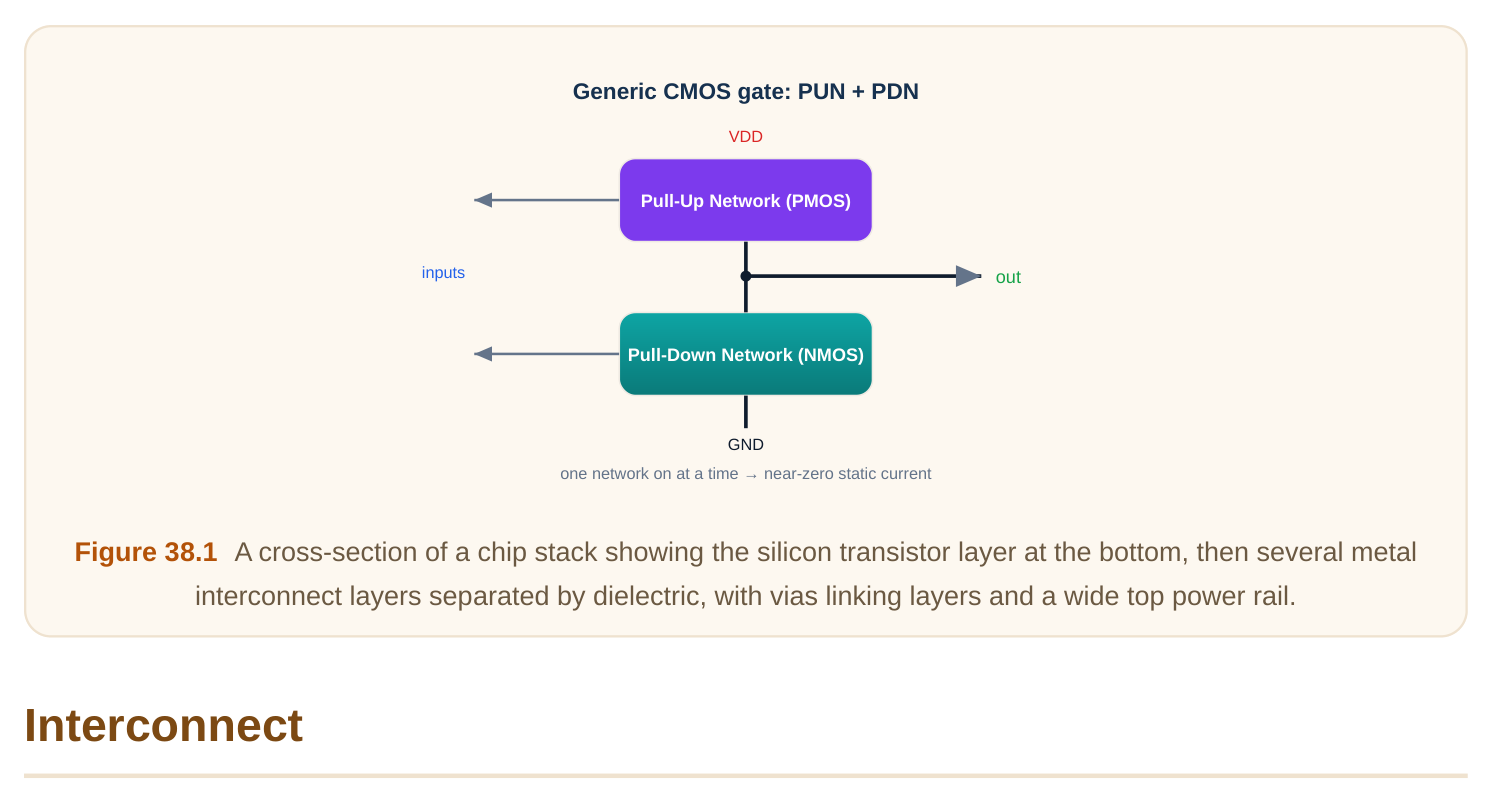
power between transistors. It is built in stacked metal layers above the silicon. Modern chips can have 12 or more metal layers.
but wires do not scale as well. Wire resistance per length rises sharply as wires get thin. So interconnect delay can dominate, sometimes over half of total path delay.
capacitance, both proportional to length. So delay rises with the square of length. A 1 mm wire might add hundreds of picoseconds without help.
into shorter segments. Since delay grows with length squared, splitting a wire cuts total delay. Repeaters can lower long-wire delay by 2x or more.
mutual capacitance. A switching aggressor can inject a glitch or shift the timing of a victim line. Spacing and shielding reduce it.
high current density over time. It can open or short a wire after years of use. Designers cap current density, often near a few mA per square micron.
supply seen by far cells and slows them. A healthy budget keeps IR drop under about 5 percent of the supply.
lower resistance, which cuts IR drop and clock skew. Signals on lower layers stay thin and dense. So power and clock distribution use the top layers.
short, and dense, linking nearby cells. Global interconnect is wide and long, spanning the chip on upper layers. Global wires carry clocks, buses, and power.
has resistance, so designers often use multiple vias in parallel. This lowers resistance and improves reliability.
Layout & Fabrication
can build reliably. They prevent shorts and broken shapes. Violating them risks yield loss or a nonworking chip.
through a mask. Each layer needs its own mask and exposure step. Feature sizes have shrunk far below the wavelength of the light used.
known timing. Cells line up in rows that share power rails. This makes automated place-and-route possible.
type. NMOS sits in a p-substrate and PMOS sits in an n-well. Wells must be tied to the proper supply to avoid latch-up.
through parasitic bipolar devices. It can destroy the chip with high current. Well and substrate taps plus guard rings prevent it.
devices. It collects stray carriers and ties the body firmly to a supply. It guards against latch-up and noise.
can damage a thin gate oxide. Long metals connected only to a gate are at risk. A small diode added to the net drains the charge.
each layer before the next is built. A flat surface keeps later lithography in focus. Dummy fill shapes are added to keep density even for CMP.
layer density uniform so CMP and etch behave evenly. It improves yield but adds parasitic capacitance.
density and chip area. A mature process may yield 80 to 90 percent on a modest die.
Memory
access transistors. The common design uses six transistors, called a 6T cell. It holds data as long as power is on.
a 1T1C cell. The charge leaks, so it must be refreshed periodically, often every 64 milliseconds. It is denser but slower than SRAM.
access transistor and junctions. Without refresh the stored bit would fade. A refresh reads and rewrites every cell within the retention window.
transistors. A bit line carries the data into or out of the selected cell. Their crossing defines a single memory cell.
and boosts it to a full logic level. It speeds reads and restores the cell value. DRAM reads are destructive, so the amplifier also rewrites.
read. During a read the access transistors disturb the internal nodes. The static noise margin during read must stay positive, often above 100 mV.
the access transistor. A higher ratio improves read stability. A common value is about 1.5 to 2.
Flash memory stores charge on a floating gate. It is used for code and persistent storage.
cache near the processor. Access times can be under a nanosecond. The cost is large area, six transistors per bit.
shrink. Variation makes small cells unreliable. This is why SRAM area scales more slowly than logic.
Clocking
can steal or add to timing margin. Designers aim to keep skew under about 5 percent of the clock period.
from supply noise and the clock source. It eats into the timing budget like skew.
flops. It is balanced so edges arrive together. An H-tree is one common balanced shape.
Since the clock is a high-activity net, this saves dynamic power. It can cut clock power by 20 to 40 percent.
and setup time, minus useful skew. In short, period is at least Tcq plus Tlogic plus Tsetup. If the period is too small, the path fails setup.
edge. So Tcq plus the shortest logic delay must exceed the hold time plus skew. Hold failures cannot be fixed by slowing the clock.
Balancing skew also helps. Unlike setup, slowing the clock does not fix hold.
slower reference. It multiplies the reference frequency and locks the phase. It is the heart of on-chip clock generation.
Low Power
power and static leakage power. Dynamic comes from charging capacitance, leakage from off transistors. Short-circuit current adds a small third part.
Slower blocks run at a lower voltage to save power. Level shifters bridge signals between islands.
needed when signals cross between voltage islands. Without it, a low-voltage high may not register correctly.
threshold. Reverse bias raises Vt to cut leakage; forward bias lowers Vt for speed. It is a runtime power-versus-speed knob.
and delay into one metric. A lower product means a better balance of speed and efficiency. It helps compare design choices fairly.
Test & Reliability
loaded and results read out. It makes internal nodes controllable and observable. It greatly raises fault coverage, often above 95 percent.
classic fault model for digital test. Test patterns aim to detect a high percentage of these faults.
the chip itself. The chip can test parts of itself without big external testers. It is common for memories.
before shipping. Weak parts fail in the factory, not in the field. It screens out infant mortality defects.
under stress over time. It makes circuits slower as they age. Designers add timing margin to cover this aging.
spikes at the pins. Clamp diodes route the surge safely to the rails. A design may target survival of a 2 kV human-body model pulse.
Design Flow
logic synthesis, then place-and-route, then timing closure and verification, then tape-out. Each step adds physical detail. Sign-off checks confirm timing, power, and rule compliance before manufacturing.
Comments
Leave a Reply