 ChipBuddy
← Home
ChipBuddy
← Home
Interview Q&A Bank — Devices & Circuits
How to Use This Bank
This bank holds short interview questions about CMOS devices and circuits. CMOS means Complementary Metal-Oxide-Semiconductor, a way to build logic using two transistor types. Read one question, hide the answer, and say your own answer out loud. Then check it. Aim for a clear twosentence reply, not a speech. Many answers carry a number, because interviewers love a candidate who can attach a quantity to a concept. Practice until the numbers feel natural.
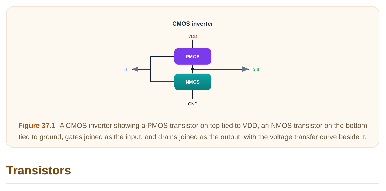
turns on with a high gate voltage and passes a strong logic 0. PMOS turns on with a low gate voltage and passes a strong logic 1. Together they form full-swing logic.
starts to conduct. A common value in older nodes is about 0.4 V. Below Vt the device is nearly off, above it the channel forms.
2 to 3 times faster than holes in the PMOS channel. So for equal drive strength, the PMOS must be made wider. A typical ratio is PMOS width about 2x the NMOS width.
above the body voltage. It happens in stacked transistors where a lower device pulls the source up. It can add 0.1 V or more to Vt and slow the stack.
slightly as drain voltage rises, even in saturation. The effective channel shortens. It is modeled by a factor lambda, often around 0.05 per volt.
when the gate is below threshold. The current drops about 10x for every 70 to 100 mV of gate decrease. This slope is the subthreshold swing.
mV per decade at 300 K. Real devices sit higher, often 80 to 100 mV per decade. Lower swing means a sharper off behavior and less leakage.
source barrier and reduces threshold voltage. It is a short-channel effect that increases leakage in tiny transistors.
voltage is small and current rises with drain voltage. In saturation the channel pinches off and current stays nearly flat. The boundary is roughly Vds equal to Vgs minus Vt.
capacitance, and the overdrive voltage Vgs minus Vt. Wider and higher overdrive gives more current. A modern device may deliver around 0.8 mA per micron of width.
channel. Thinner oxide gives stronger gate control and more current. Modern equivalent oxide thickness is near 1 nm, which raises tunneling leakage.
on three sides. This gives better control and less leakage than a flat device. It became common around the 22 nm and 16 nm nodes.
Inverter & Gates
output to 0. When the input is low, the PMOS turns on and pulls the output to 1. Only one network conducts in steady state, so static current is near zero.
voltage where input equals output. With matched drive it sits near VDD/2, for example 0.5 V on a 1.0 V supply. Sizing the PMOS wider shifts Vm upward.
no direct path links VDD to ground. The only static current is leakage. This is why CMOS replaced older logic that burned constant current.
output flips wrongly. High and low margins are measured at the unity-gain points of the transfer curve. A healthy margin is around 0.3 to 0.4 V on a 1.0 V supply.
PMOS in parallel to VDD. The output is low only when both inputs are high. Because of the series stack, the NMOS devices are sized wider to keep speed.
PMOS in series to VDD. The output is high only when both inputs are low. The series PMOS stack makes NOR slower than NAND, so NAND is preferred.
slow PMOS in series. Since PMOS is already weaker, stacking it hurts more. So NAND-based logic is usually faster for the same area.
connects the output to VDD. The pull-down network is the NMOS part that connects the output to ground. They are logical complements of each other.
switch. It passes both strong 1 and strong 0 because the two devices cover each other's weakness. It needs both the control signal and its complement.
Delay & Sizing
output crossing 50 percent. It is often split into rise delay and fall delay. A small gate in a modern node may show tens of picoseconds.
capacitance. Delay is roughly 0.69 times R times C. If R is 5 kilo-ohm and C is 10 femtofarad, delay is about 35 picoseconds.
load capacitance and more delay. A common rule keeps fan-out near 4 for good speed.
process-independent speed yardstick. In a given node it might be around 15 to 20 picoseconds.
inverter of equal output current. An inverter has logical effort 1. A 2-input NAND has about 4/3, and a 2-input NOR about 5/3.
stage. But the wider gate adds input capacitance that loads the prior stage. The best size balances the two, often near a stage effort of 4.
about 4, near the number e times its delay sense. So the optimal stage count is about the natural log of the total load ratio divided by ln(4). For a 64x load this gives roughly 3 stages.
10 and 90 percent levels. Slow slew increases delay and short-circuit power. Designers often keep slew under about 100 picoseconds.
direct path from VDD to ground. This wastes power and is worse with slow inputs. It usually adds under 10 percent of total dynamic power if slews are sharp.
and branching effort along the path. Delay grows with the total effort. Minimizing it means spreading effort evenly across stages.
Power
It equals alpha times C times V squared times f, where alpha is the switching activity. At 0.9 V, 50 fF, and 1 GHz with alpha 0.2, it is about 8 microwatts.
and the energy of that charge is C times V squared. So halving the supply cuts dynamic power by about 4x. This makes voltage the strongest power lever.
mainly from subthreshold and gate-oxide leakage. In advanced nodes it can be 20 to 40 percent of total power.
node switches. A clock has alpha near 1, while random logic may sit near 0.1 to 0.2. Lower activity means lower dynamic power.
switch. This removes leakage during sleep. It can lower idle leakage by 10x or more but adds wake-up latency.
leak less but switch slower, used on non-critical paths. Low-Vt cells go on the few timing-critical paths.
frequency when full speed is not needed. Since power follows V squared times f, the savings are large. Dropping from 1.0 V to 0.8 V can cut power by roughly 40 percent.
Sequential
clock edge. A common design uses two latches in a master-slave pair. It holds one bit between clock edges.
data while the clock is at one level. A flip-flop is edge-sensitive and captures only at the clock edge. Flip-flops are easier to time in synchronous design.
changes too late, the flip-flop may capture the wrong value. A typical setup time is 30 to 60 picoseconds.
violation lets new data race through and corrupt the captured bit. Hold times are often small, near 10 to 20 picoseconds.
adds to the path delay between flip-flops. A value of 40 to 80 picoseconds is common.
setup or hold violation. It resolves randomly after an unpredictable time. Synchronizer chains reduce its odds to acceptable levels.
an asynchronous signal into a clock domain. The extra stages give metastable states time to settle. Two stages are common, three for high-reliability designs.
Circuit Families
that always define the output. It is robust, low-leakage, and easy to design. It is the default style for most logic.
conditionally discharges it during evaluation. It is fast and compact but sensitive to noise and leakage. It needs careful clocking.
stages can cascade. The inverter keeps signals monotonic during evaluation. It trades extra area for cascadability.
instead of full pull networks. It can use fewer transistors for some functions like multiplexers. The drawback is weakened logic levels.
maximum speed in a wide function like a fast adder. It uses fewer transistors on the critical path. But accept higher design effort and lower noise margins, often costing 20 to 30 percent more verification time.
Comments
Leave a Reply