 ChipBuddy
← Home
ChipBuddy
← Home
Cell Delay, Slew & the Timing Library
Chapter 2 — Cell Delay, Slew & the Timing Library
Static timing analysis (STA) adds up many small numbers. It is only as good as those numbers. Every arrival time comes from them. Every slack value comes from them too. (Slack is the spare time a path has.) All these numbers come from one place. That place is the timing library (a file of pre-measured cell data). You must know how one cell's delay is measured. You must know how it is stored. Without that, STA is a black box. This chapter opens the box. We look at what sets a gate's delay. We look at how that is saved as small data. We look at how the tool reads it back. We also see where the simple model fails on tiny chips.
What Actually Determines a Cell's Delay
A signal change arrives at a gate's input. The transistors switch. The output node is driven. The time the output takes to respond is not fixed. It depends mainly on two things.
- Input slew (also called input transition time): how fast the input signal changes. A sharp edge switches transistors fast. A slow edge keeps them half-on longer. A slow edge makes the delay longer.
- Output load: the total capacitance the gate must drive. (Capacitance is the charge a node can hold.) More load means more charge to move. More charge means a slower edge and a longer delay.
These two factors rule normal logic cells. The link is non-linear both ways. That is why we cannot store one delay number per cell. Picture a small gate driving a tiny load with a crisp input. Now picture the same gate driving a long, heavy wire with a lazy input. They behave very differently.
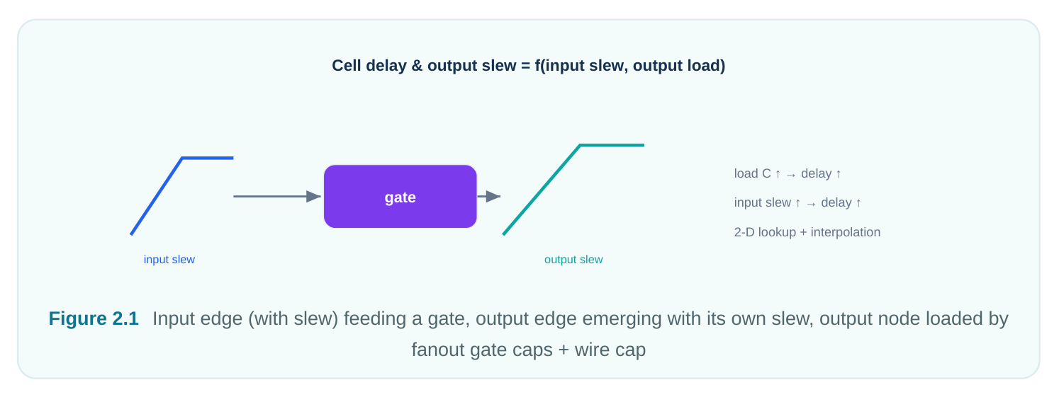
Two output values are measured. Both depend on the same two inputs.
- 1. Cell delay — measured from the input crossing a threshold (often 50% of the rail) to the output
crossing its threshold.
- 2. Output transition (slew) — how fast the output edge is. It is usually measured between two
voltages, such as 10% and 90% of the rail. It is then scaled to a full swing. The second output matters a lot. It becomes the input slew of the next gate. So delay and slew always travel together.
The Lookup-Table (NLDM) Delay Model
The most common method stores delay and output slew as two-dimensional lookup tables. During library setup, the cell is simulated. (A transistor-level simulator does this.) It runs across a grid of inputslew values and output-load values. Each grid point gives one delay and one output slew. The result is a pair of tables per timing arc. A delay table looks like this. Values are illustrative, in picoseconds.
| input slew \ output cap | 2 fF | 8 fF | 24 fF | 96 fF |
|---|---|---|---|---|
| 6 ps | 14 | 25 | 52 | 150 |
| 24 ps | 22 | 33 | 60 | 162 |
| 96 ps | 40 | 52 | 80 | 188 |
| 360 ps | 82 | 96 | 130 | 244 |
The tool needs the delay for a real point. Say the input slew is 30 ps and the load is 12 fF. That point rarely lands on a grid line. So the tool interpolates. (Interpolate means estimate between known points.) It blends the four nearest table entries. This is usually bilinear. If the point falls outside the grid,
the tool extrapolates instead. (Extrapolate means guess beyond known points.) That is less accurate. It is a common cause of warnings. A good library picks grid ranges that cover real use. Then extrapolation is rare. This scheme is called a non-linear delay model. The stored surface is non-linear. The blend between points is linear.
RISE VS FALL ARCS
A gate is not the same for rising and falling edges. The pull-up transistors and pull-down transistors differ. They differ in strength and shape. So each arc stores separate tables for a rising output and a falling output. The tool tracks edge direction through the path. It picks the matching table at each gate.
UNATENESS
Each combinational arc records a rule. The rule links output edge direction to input edge direction. This property is unateness.
- Positive unate — a rising input gives a rising output. A falling input gives a falling output. Examples are a buffer, an AND, an OR. The edge direction is kept.
- Negative unate — a rising input gives a falling output, and the reverse. Examples are an inverter, a NAND, a NOR. The edge direction flips.
- Non-unate — the output direction cannot be told from one input alone. It depends on the other inputs. Examples are an XOR or XNOR. Both directions must be checked. Unateness tells the tool which output edge goes with a given input edge. This is needed to build max (setup) and min (hold) paths correctly.
Timing Arcs: What the Library Stores
A timing arc is a measured link between two pins of a cell. There are two main families. Combinational arcs join an input pin to an output pin through the logic. They carry the delay and slew tables above. They are tagged by edge and unateness. Sequential arcs describe a flip-flop or latch. They come in three kinds.
- Clock-to-Q (propagation) arc — from the active clock edge to the data output. This is a real delay arc. It has its own delay and slew tables. They are indexed by clock slew and Q load.
- Setup constraint arc — the least time data must be steady before the clock edge. It is stored as a constraint table. It is usually indexed by data slew and clock slew. It gives a requirement, not a delay.
- Hold constraint arc — the least time data must stay steady after the clock edge. It is tabulated in the same way. The table below sums up the arc types.
| Arc type | From → To | What it stores | Used for |
|---|---|---|---|
| Combinational | input → output | delay + output slew tables (rise/fall, | path delay propagation |
unate)
Clock-to-Q clock → Q/QN delay + output slew tables launch of captured
| Setup | data → clock | constraint value (table) | setup (max) check |
|---|---|---|---|
| Hold | data → clock | constraint value (table) | hold (min) check |
| Recovery/ | async pin → | constraint value Removal | async control timing clock |
Setup and hold values change with slew. That is why they are tabulated, not stored as one number. A slow data edge needs more setup margin than a sharp one.
Per-Cell Library Data
The library holds more than arcs. Each cell entry carries support data. The tool needs it to compute load and check signals.
| Data item | Meaning | Why STA needs it |
|---|---|---|
| Input pin capacitance | cap each input shows to its driver | becomes part of the next stage's |
output load
| Output drive / arc tables | the delay/slew surfaces above | computes this cell's contribution |
|---|---|---|
| Max capacitance | largest load the output may legally drive | design-rule (DRV) checking |
| Max transition | slowest edge allowed on a pin | DRV checking; guards model |
validity
| Max fanout | logical fanout limit | DRV checking |
|---|---|---|
| Function | Boolean equation of the cell | sense/unateness, debugging |
| Operating conditions | process/voltage/temperature of the | corner selection |
characterization
Area, leakage, internal physical/power attributes downstream optimization
HOW OUTPUT LOAD IS COMPUTED
The load an output drives has two parts.
- 1. Pin capacitance of every gate input it feeds. This is read from each receiver's library entry.
- 2. Wire (net) capacitance of the wire between them. This comes from an estimate before routing.
After routing it comes from extraction. (Extraction means measuring real wire values from the layout.) So load = sum of receiver input caps + net cap. Early on, wire cap is estimated from a simple fanout-based model. After place-and-route it comes from parasitic extraction. Extraction also adds wire resistance. That resistance is what strains the simple table model.
Why the Table Model Strains at Advanced Nodes
The lookup-table model assumes the load is one lumped capacitor. That holds when wires are short. Then resistance is tiny. On tiny chips this stops holding.
- Wires become resistive. The net acts like a spread-out RC network, not a clean capacitor. (RC means resistance plus capacitance.) The driver "sees" a shielding effect. Near capacitance charges fast. Far capacitance lags behind.
- Edges become very sharp. The next gate's input may start switching before the driver edge finishes. One delay-from-threshold number can no longer catch this.
- The real voltage shape at a receiver can wobble or have a long tail. A single slew value cannot show that. To use a table on a resistive net, tools first shrink the RC network. They reduce it to one effective capacitance. (This is one value that copies the driver's switching behavior.) Then they look up the table with that value. It is a handy estimate. But it throws away the wave shape.
Current-Source Models: Modeling the Driver as a Current Source
The more accurate way treats the output as a current source. (A current source pushes out current.) The output current depends on the output voltage and the input over time. The library does not store "delay vs slew vs cap." Instead it stores how much current the driver gives as the output voltage changes. It often stores the driver's internal caps too. The reward is large. The tool can push this current-source model into the real spread-out RC network. It then solves for the true voltage shape at each receiver pin. This catches resistive shielding, long tails, and sharp-edge effects. The lumped-cap table simply cannot. The cost is bigger libraries, longer setup, and heavier compute during analysis.
| Model | What it captures | Net handled as | Relative accuracy |
|---|---|---|---|
| Linear / first-order | delay ≈ k·load; one slope | lumped cap | low — legacy/estimation |
only
| Non-linear lookup | delay & slew vs (input slew, cap) | lumped (or effective) | good at older/relaxed |
|---|---|---|---|
| table | cap | nodes | |
| Table + effective- | table driven by RC-reduced cap | distributed RC, cap | better on resistive nets reduced |
| Current-source | full output-current behavior, real model | full distributed RC waveform | highest — advanced nodes |
Here is the practical advice. Table models are fine for many designs. They run faster too. Currentsource models win when net resistance and sharp edges make wave shape matter. A flow can use both. Quick early runs may use tables. Final signoff may use the current-source model.
Slew Propagation and Why Degradation Matters
Each stage outputs a delay and an output slew. That output slew becomes the next stage's input slew. This chains down the whole path.
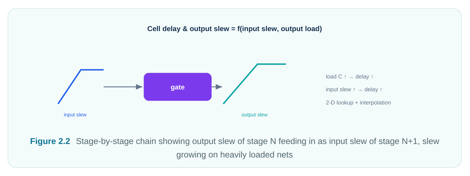
Slew degradation is the trend of edges getting slower. They degrade as they pass through heavy or resistive stages. It matters for three reasons.
- 1. A slower input slew raises the next cell's delay. So slew trouble piles up along a path. It does not
stay local.
- 2. Setup and hold values grow with worse slew. That eats into margin.
- 3. Very slow edges break max-transition rules. They can cause signal problems too. Examples are
crowbar current and more crosstalk. This is why STA does not move delay alone. It moves the (delay, slew) pair together. It recomputes each one at every node. It uses the upstream slew and the local load. Get slew wrong early and every later delay is quietly wrong too.
Code: Reading Libraries and a Conceptual Delay Lookup
The first sketch shows commands to load libraries and inspect cells. These commands are toolspecific. They are not part of the SDC standard. So they are marked illustrative.
# illustrative — generic, not tool-specific
# load characterized libraries for the corners we will analyze
read_liberty  ./libs/stdcells_slow_0p70v_125c.lib   ;# illustrative
read_liberty  ./libs/stdcells_fast_0p90v_m40c.lib   ;# illustrative
# inspect a cell's arcs, pin caps, and design-rule limits
report_cell_timing   NOR2_X1                         ;# illustrative
report_pin_capacitance  NOR2_X1/A                    ;# illustrative
report_lib_limits   -max_transition -max_capacitance ;# illustrative
The SDC-standard part of an STA setup is about constraints. It is not about library reads. For contrast, these are real standard commands.
# standard (SDC)
create_clock -name CLK -period 2.5 [get_ports CLK]
set_input_transition  0.06 [get_ports din*]   ;# drives input-slew lookup at first
stage
set_load              0.012 [get_ports dout*] ;# output cap for boundary cells
set_max_transition    0.35 [current_design]   ;# DRV ceiling checked against
propagated slew
The second sketch is pseudo-code. It shows how a tool does one delay lookup at an arc. It uses bilinear interpolation between four nearby grid points. This models the algorithm. It is not a runnable command.
# illustrative — generic, not tool-specific (conceptual algorithm)
proc lookup_delay {table in_slew out_cap} {
# find bracketing rows (slew) and columns (cap)
lassign [bracket $table rows $in_slew] s_lo s_hi
lassign [bracket $table cols $out_cap] c_lo c_hi
set d00 [cell $table $s_lo $c_lo] ; set d01 [cell $table $s_lo $c_hi]
set d10 [cell $table $s_hi $c_lo] ; set d11 [cell $table $s_hi $c_hi]
# interpolation weights along each axis
set ws [expr {($in_slew - $s_lo) / ($s_hi - $s_lo)}]
set wc [expr {($out_cap - $c_lo) / ($c_hi - $c_lo)}]
# bilinear blend of the four corners
set top [expr {$d00 + $wc*($d01 - $d00)}]
set bot [expr {$d10 + $wc*($d11 - $d10)}]
return  [expr {$top + $ws*($bot - $top)}]
}
# the same routine, run on the slew table, yields the output slew
# that becomes in_slew for the next stage (slew propagation)
Note one thing. The same routine runs on the output-slew table. It then gives the value passed to the
next stage. That is the mechanism behind slew propagation above.
Interview Q&A
linear function of two variables. Those are input slew and output load. Neither stays constant in a real design. One number would be right for only one operating point. A grid lets the tool interpolate the right delay for each instance.
direction to its input edge direction. Positive unate keeps polarity. Negative unate flips it. Non-unate depends on other inputs. The tool needs it to pick the right rise or fall table. It also needs it to build worst-case max and min paths. Get it wrong and you pick the wrong edge and the wrong delay.
wire resistance and sharp edges break the lumped-capacitor assumption. This is typical on advanced nodes with long, resistive nets. The table model shrinks the load to one capacitance. It cannot show resistive shielding or wave tails. A current-source model drives the real RC network and solves for the true waveform. That gives signoff-grade accuracy. The cost is size and runtime.
edges through loaded or resistive stages. It compounds because each output slew becomes the next input slew. A slower input slew raises the next cell's delay and its constraints. So a slew problem early in a path inflates every later delay. It does not stay local. That is why STA always moves the (delay, slew) pair together.
Key Takeaways
- A cell's delay and output slew depend on input slew and output load. Both are measured by transistor-level simulation and stored per arc.
- The non-linear lookup-table model holds these as 2-D tables indexed by input slew and load. The tool interpolates and warns on extrapolation. Each arc has separate rise/fall tables and an unateness tag.
- Timing arcs are combinational (delay tables) and sequential (clock-to-Q delay tables plus setup/ hold constraint tables). Constraints are tabulated because they too change with slew.
- Output load = receiver pin caps + net cap. Wire cap is estimated pre-route and extracted post- route. Extraction's wire resistance is what strains lumped-cap models.
- Current-source models treat the driver as a current source driving the real RC net. They catch wave effects the table model cannot. They are the accuracy choice at advanced nodes.
- Slew propagates alongside delay. Slew degradation compounds down a path. So accurate early slew is vital to every later number.
Comments
Leave a Reply