 ChipBuddy
← Home
ChipBuddy
← Home
Power-Aware & Multivoltage STA
Timing a Chip That Runs at Many Voltages
Modern low-power chips do not use one supply voltage. Different blocks live in different voltage domains (areas with their own supply). Some blocks change their voltage while running. This is called DVFS (dynamic voltage and frequency scaling). Other blocks turn off completely. Every one of these choices changes delay. Delay depends heavily on supply voltage. So timing analysis must know the power plan, not just the netlist (the list of cells and wires). This chapter explains what changes in STA (static timing analysis) when many voltages, special cells, and shutdown are used.
Voltage's Effect on Delay, and Why Each Domain Needs Its Own
Library
Cell delay grows fast as supply voltage drops. The link between voltage and delay is not a straight line. It bends sharply near the threshold (the voltage where a transistor just turns on). Think of voltage like water pressure. Low pressure means water flows slowly. Low voltage means signals settle slowly. A library (a file of cell timing data) made at one voltage cannot serve a block at another voltage. The numbers would be wrong. So each domain carries its own library views, made at that domain's voltage. STA must attach the right view to the right cells. This grows the corner space. A corner is one mix of voltage, process, and temperature. Say a design has three supplies. Say each supply can sit at two operating points. Add the usual process and temperature spread. You now get far more views than a single-voltage chip. The setup job is to list only the voltage mixes that can truly happen together. Do not list every possible combination.
| Item | Single-voltage STA | Multivoltage STA |
|---|---|---|
| Library views | one per PVT | one per (domain-voltage, PVT) |
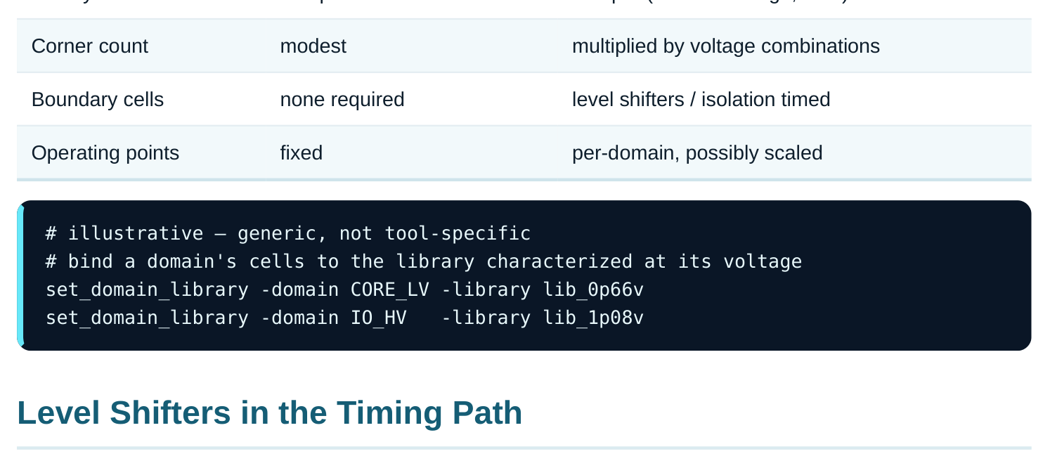
A signal may leave a low-voltage domain and enter a higher-voltage one. A low '1' may not register right without help. A level shifter (a cell that rebuilds the signal at the new voltage) fixes this. The reverse direction has its own concerns. To STA, a level shifter is just a cell with timing arcs (input-to-output delay paths). But it is a required cell on a voltage crossing. Two things matter:
- 1. Its delay must be in the path. The shifter adds real delay. Forgetting one corrupts the crossing's
timing.
- 2. It must be characterized for the right voltages. An up-shifter's delay depends on both the source
and the destination rail. So it needs correct dual-rail library data.
Worked example — a domain crossing
A path leaves a 0.66 V domain. It enters a 1.08 V domain through an up-shifter. The launch-side logic adds 0.95 ns. It is slow because 0.66 V is slow. The level shifter adds 0.21 ns. The capture-side logic adds 0.34 ns. The total data path is 0.95 + 0.21 + 0.34 = 1.50 ns. The shifter is timed against the capture clock in the 1.08 V domain. Drop the shifter from the model and you lose 0.21 ns. You also mis-time the crossing. This is a classic multivoltage STA bug.
| Crossing | Cell required | STA must |
|---|---|---|
| Low → high V | up level shifter | include delay, dual-rail char |
| High → low V | down shifter (often) | include delay |
| Same V, can power down | isolation cell | time enable, model clamp |
Isolation, Always-On Logic, and Shutdown Domains
A domain may power down. Signals leaving it pass through isolation cells. These cells clamp the signal to a safe value. STA has these jobs:
- Time the isolation enable. It works like any control signal. It must settle before the domain powers down. It must be driven from an always-on supply.
- Model the clamp. Then timing during shutdown is analyzed right.
- Bind always-on cells to the right rail. Some cells must keep working during shutdown. These include isolation control, retention control, and certain level shifters. They draw from a separate always-on rail. STA must bind them to that rail's library, not the switched one.
- Treat power states as modes. The design has named states, such as all-on, domain-X-off, and sleep. Each state is a mode with its own active domains and clocks. Timing must hold in every reachable state. It must also hold during the moves between states.
# illustrative — generic, not tool-specific# analyze each power state as its own modeanalyze_power_state -state ALL_ONanalyze_power_state -state ACCEL_OFFreport_timing -mode ACCEL_OFF -delay setup
| Special cell | Powered by | STA concern |
|---|---|---|
| Isolation | always-on | enable timing, clamp model |
A retention flop keeps key state alive on an always-on supply. The rest of the domain goes dark. STA here is mostly about the control timing. The save and restore signals must be ordered right. They must line up with isolation and the power switch. STA also confirms the retention cells use the always-on supply. The functional order is fixed: isolate, then save, then power down. To wake up: power up, then restore, then de-isolate. A structural check confirms this order. But each control-path delay is an STA check.
DVFS lets a domain change its voltage and clock while running. It trades speed for power. Each operating point is its own timing context. A high-performance point uses high voltage and a fast clock. A low-power point uses low voltage and a slow clock. Both must close (pass timing). Here is the tricky part. The worst setup corner and the worst hold corner can sit at different operating points. A level shifter's needed direction can even flip between points. So sign-off lists the operating points as scenarios. It then takes the worst across them. This is the same multi-corner, multi-mode method, now driven by voltage as well as PVT.
| DVFS point | Voltage | Clock | Typically worst for |
|---|---|---|---|
| Turbo | high | fast | setup (tight period) |
| Nominal | mid | mid | balanced |
| Low-power | low | slow | hold (fast logic vs skew), leakage |
Interview Q&A
voltage, and not in a straight line. A block at 0.66 V is far slower than one at 1.08 V. Each domain needs library views made at its own voltage. The wrong view gives wrong delays.
arcs. Its delay must be in the path. It must be characterized for both source and destination rails. Omitting or mis-modelling it corrupts the crossing.
down. The enable must come from an always-on supply. STA also checks that the clamp is modelled so shutdown-state timing is right. The order is checked structurally. The control delays are STA checks.
domains, clocks, and constraints. So timing must be checked per state and across transitions. It is the same multi-mode method, indexed by power state.
slows, which eases setup. But hold depends on skew and minimum delay, not the period. Fast mindelay paths plus skew can still break hold. So the low-power point often dominates hold while turbo dominates setup.
Key Takeaways
- Delay depends strongly on supply voltage, so each domain carries library views made at its voltage, growing the corner space.
- Level shifters on voltage crossings are required timed cells needing dual-rail characterization; omitting them is a classic bug.
- STA times the control of isolation and retention (enable, save, restore) and binds always-on cells to the always-on rail.
- Each power state is a mode; timing must hold in every reachable state and transition.
- DVFS operating points are scenarios; worst setup and worst hold can occur at different voltages, so sign off across all of them.
Comments
Leave a Reply