 ChipBuddy
← Home
ChipBuddy
← Home
Interconnect Delay & RC Parasitics
Long ago, a wire was just a wire. It linked one pin to another. It added no delay. Back then, timing was only about logic gates. That world is gone. Today, chips use tiny process nodes (very small transistor sizes). The metal wire between two cells is now a real object. It has resistance (opposition to current flow). It also has capacitance (ability to store charge). Together these can dominate a path's delay. An STA (Static Timing Analysis) engineer must respect wires. Ignore them, and your chip passes on paper but fails in silicon. This chapter gives you the mental model for wire delay.
Why Wire Delay Matters as Much as Cell Delay
Three physical trends make wires a first-class concern. First, resistive wires. Smaller chips mean narrower, thinner metal. Resistance rises as the wire's cross-section shrinks. So each new node makes a wire more resistive per unit length. Meanwhile, transistors got faster. So a signal now spends more time in metal than in gates. Second, large fanout and long routes. Fanout means how many sinks a net drives. A net with many sinks gathers lots of capacitance. A long net gathers capacitance from every micron of metal. The driver must charge and discharge all of it. Far sinks then see a late, weak signal. Third, coupling. Neighboring wires sit very close. The capacitance between them can match or beat the capacitance to ground. This coupling causes crosstalk (one wire disturbing another). We study crosstalk later. Here, it just adds load.
There is a deeper scaling story too. Gate delay improves with each shrink. The transistor gets smaller and faster. Wire delay does not cooperate. A narrower wire has more resistance. A wire closer to neighbors has more coupling capacitance. So the resistance-capacitance product of a fixed-length wire can get worse each generation. Designers fight back. They use thicker upper metal layers. They insert repeaters (buffers that refresh a signal). They plan net shapes carefully. But the physics will not go away. So always ask two questions. How fast is the gate? And what must it drive, and how resistive is the path?
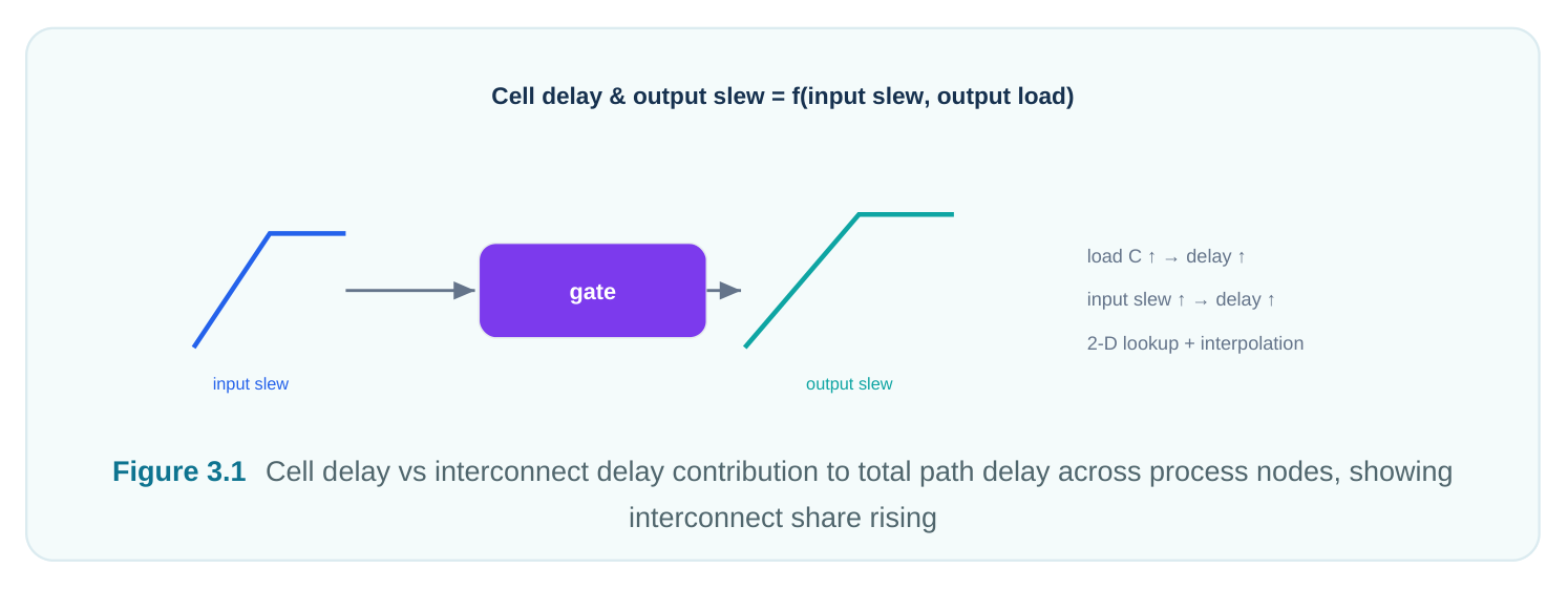
Here is the practical result. A path's delay is the sum of two arc types. Cell arcs go from a gate's input pin to its output pin. Net arcs go from a driver's output pin to a receiver's input pin. At advanced nodes, net arcs are not tiny. On long, busy, resistive nets, a net arc can beat the cell delay that feeds it.
Modeling a Net: From Lumped-C to Distributed RC
A net is one continuous physical object. But STA needs a discrete electrical model to compute delay. There is a ladder of models. Each one trades simplicity for accuracy. Lumped capacitance (lumped-C). This is the simplest model. It treats the whole net as one capacitor on the driver. Wire resistance is ignored. The driver sees one capacitance. It equals all the wire and pin capacitance added up. This is fast. It works when resistance is small. That means short nets, or early planning before any routing exists. Lumped RC. This is one step up. The net becomes one resistor in series with one capacitor. It shows that resistance adds delay. But it cannot show where the resistance and capacitance sit. So it is a rough fit for any branching net. Distributed RC (pi-models and RC trees). This is the faithful model. It cuts the net into many small pieces. Each piece has its own series resistance and shunt capacitance. One piece is often drawn as a pi-model. Here the capacitance is split on both sides of a resistor (C/2 — R — C/2). Chain these pieces. Branch them at every fork. You now have an RC tree. It is rooted at the driver. It has resistance on every edge. It has capacitance at every node. It ends at the receiver pins. This is what real extraction makes. It is what accurate delay calculation uses.
Modeling a net: increasing fidelity
lumped C lumped RC distributed RC (π / tree)
| Model | What it captures | When it is adequate |
|---|---|---|
| Lumped-C | Total capacitive load only | Short nets; early floorplanning; |
resistance negligible
Lumped RC One R and one C, no spatial detail Quick estimates; nets where one
| Distributed RC (pi / | Resistance and capacitance distributed along | Sign-off; long, resistive, or high-fanout |
|---|---|---|
| RC tree) | the net, branching, per-sink delays | nets at advanced nodes |
Here is the rule of thumb. The more wire resistance matters, the lower you go in this table. At nanometer nodes, sign-off lives in the bottom row.
Elmore Delay: The Intuition Behind RC Trees
You need not memorize the exact delay solver. But you must grasp why delay builds up in an RC tree. The classic mental model is Elmore delay. Picture the driver at the root. Pick a receiver somewhere downstream. Walk the one path from root to that receiver. For each resistor on that path, do one thing. Multiply it by all the capacitance downstream of it. That means every capacitor it must help charge through itself. Add up these products. That sum is the Elmore delay to that node. The key idea is resistance × downstream capacitance. A resistor near the driver carries current for the whole net. So it gets multiplied by a large downstream capacitance. It contributes a lot. A resistor near a leaf charges only the small capacitance past it. So it contributes little. This explains three things.
- Delay grows roughly with the square of wire length. Double the length, and you roughly double both the resistance and the capacitance it charges.
- Different sinks on one net have different delays. A near sink and a far sink share a driver. But they see very different built-up R×C.
- Buffering long nets helps a lot. A buffer resets the R×C build-up. It breaks one quadratic term into two smaller ones. Elmore is a first-moment estimate. It tends to be pessimistic. It ignores the waveform shape. But its intuition is exactly right. It explains most of what you see in real reports.
A small worked example makes this clear. A net leaves a driver through a resistor R1 of 15 ohms. It reaches an internal node. There it splits. A resistor R2 of 10 ohms goes on to a far sink with capacitance C2 of 4 fF. A capacitance C1 of 6 fF sits at the internal node. The Elmore delay to the far sink is R1 times the total downstream capacitance (C1 + C2), plus R2 times only C2. So that is 15 × (6 + 4) + 10 × 4 = 150 + 40 = 190 in fF-ohm units. R1 is multiplied by everything past it. All the net's current flows through it. R2 is multiplied only by C2. Nothing lives past it. Now ask for the near sink hanging right off the internal node. R2 and C2 drop out. Its delay is just 15 × 10 = 150. Same net, smaller number. This is why one net gives a different delay for each receiver. It is why real tools report per-pin arrival times, not one delay per net.
Parasitic Extraction: Pre-Route Estimates vs Post-Route Reality
The R and C values feeding these models come from parasitic extraction. This is the act of computing electrical parasitics from physical shapes. There are two very different regimes. Pre-route estimates. Before detailed routing exists, the tool has no real metal to measure. So it guesses. Older flows used wire-load models. These are statistical tables. They map a net's fanout (and sometimes block size) to an estimated R and C. They are crude. Every net of a given fanout gets the same parasitics. The real sink locations do not matter. Modern placement-aware flows do better. They use virtual-route (or trial-route) estimation. The tool sketches a likely route from real pin locations. It estimates parasitics from that shape. Both are still predictions. They guide synthesis and placement. They are not trustworthy for sign-off. Post-route extracted parasitics. Once routing is done, an extraction tool reads the real metal. It sees each segment's width, length, layer, and nearby neighbors. It then computes real R and C. These go into a standard parasitic exchange format (a parasitic netlist file). The timing tool annotates them onto the design. They reflect real silicon shapes. So post-route extracted parasitics are the trustworthy numbers for sign-off.
| Stage | Source of parasitics | Accuracy | Typical use |
|---|---|---|---|
| Pre-place / | Wire-load model (fanout-based | Lowest synthesis | Logic synthesis guidance statistics) |
| Post-place / pre- | Virtual-route / trial-route estimate | Moderate route | Placement and early optimization |
| Post-route | Full extraction of real geometry | Highest | Timing sign-off |
A common interview theme is this. Why does timing change between synthesis and post-route? Because the parasitics changed. They went from a statistical guess to measured reality. Paths that looked fine on wire-load models can blow up once real, resistive routing is extracted. It helps to know what extraction really measures. Resistance comes from each segment's shape. It is length divided by cross-section, scaled by the layer's sheet resistance. Add via resistance at every layer change. Capacitance comes in three flavors. Area capacitance goes to the planes above and
below. Fringe capacitance comes from the wire's edges. Lateral coupling capacitance goes to neighbors on the same layer. Extraction engines differ in accuracy. Fast rule-based methods look up precomputed capacitance-per-length tables by shape. Field-solver methods solve the real 3D electrostatics. These are saved for the most critical nets. The output is the same kind of parasitic netlist either way. Sign-off quality needs an accuracy the foundry has correlated against silicon.
Slew Degradation and the Effective Capacitance Concept
A resistive net does more than add delay. It also degrades the slew (transition time) as the signal travels. The driver may launch a sharp edge. But resistance acts like a filter. It slows the rate of change. By the time the edge reaches a far sink, it is much more gradual than at the driver. Cell delay depends on input slew. (Recall the nonlinear delay model from the last chapter.) So a slow slew at a receiver makes that receiver's delay worse. Slew degradation thus carries pessimism downstream, net by net. This same resistance leads to a key and often misunderstood idea. It is effective capacitance. You might think the driver must charge the net's total capacitance. It does not. The wire's resistance shields the far capacitance from the driver. This happens during the critical early part of switching. Think of pouring water through a long thin pipe. The far end fills slowly. The near capacitance responds at once. But resistance slows current to the far capacitance. So the driver effectively sees less than the total C.
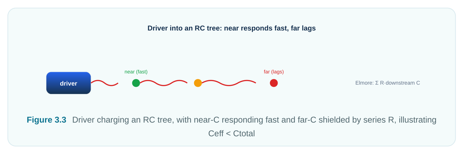
Delay tools handle this with an effective capacitance (Ceff). It is one equivalent capacitance. If it replaced the whole RC tree, it would give the same driver delay. Ceff is always less than or equal to the total capacitance. The more resistive the net, the more shielding, and the smaller Ceff gets versus Ctotal. The tool iterates. It guesses Ceff. It computes the driver's output waveform. It recomputes Ceff from that waveform. It repeats until the value settles. This understanding stops a classic mistake. Do not assume a driver's delay scales with total net capacitance. On a resistive net it scales with Ceff. The interconnect delay to the sinks is a separate term across the RC tree.
How Net Delay Enters the Timing Graph
Recall that STA models the design as a timing graph. It has nodes (pins) joined by arcs. Interconnect enters this graph as net arcs. For each driver-to-sink link, the delay tool produces three things.
- A cell arc delay through the driving gate. It uses the input slew and the net's effective capacitance as the load.
- A net arc delay from the driver output pin to each receiver input pin. It comes from the RC tree (the R×C build-up to that sink).
- A slew value at each receiver pin. The net degrades it. It becomes the input slew for the next cell arc. The path delay is then the alternating sum of cell arcs and net arcs. It runs from launch to capture. Each sink has its own net-arc delay and its own degraded slew. So one multi-fanout net adds differently to every path through it. This is why one number per net cannot summarize interconnect. The timing graph carries per-sink detail.
Cell vs Interconnect Delay Contributors
It helps to keep straight what drives each kind of delay.
| Delay component | Primary contributors | What reduces it |
|---|---|---|
| Cell (gate) delay | Drive strength, input slew, effective load (Ceff), Vt flavor, PVT | Larger/faster cell, lower Vt, better input slew, lower load |
| Interconnect (net) | Wire R and C, net length, fanout, | Buffer insertion, shorter routes, wider/ |
| delay | branching, layer choice | upper-layer metal, less fanout |
| Slew at receiver | Driver strength vs Ceff, net resistance | Stronger driver, less resistive net, buffering |
shielding Notice the levers differ. You fix a cell delay by changing the gate. You fix an interconnect delay by changing the wire. That means rerouting, buffering, upsizing metal, or splitting fanout. So first find which kind of problem you have. The report's split between cell and net delay tells you at once.
Conceptual Code: Annotating Parasitics and Reporting Net Delay
The first block shows the standard sign-off intent. Read extracted parasitics. Then report path delay with the cell/net split visible. The constraint-style and reporting commands follow widely used conventions.
# Annotate post-route extracted parasitics onto the design,
# then run timing and inspect the cell-vs-net delay split.
# read_parasitics is the standard concept: load the extracted
# RC data (parasitic exchange format) produced after routing.
read_parasitics  ./extracted/top.spef            ;# standard concept (parasitic
exchange format)
# Report a path and show the breakdown of cell vs net (interconnect) delay.
# -input_pins / showing net arcs is the standard reporting intent.
report_timing -delay_type max \
-path_type full \
-input_pins                          ;# standard (SDC-style reporting)
The second block is illustrative pseudocode for the Elmore intuition. It is generic, not a real tool command. It makes the R×downstream-C build-up concrete.
# illustrative -- generic, not tool-specific
# Elmore delay to one sink: sum over resistors on the
# root-to-sink path of (R * total downstream capacitance).
proc elmore_delay {root sink rc_tree} {
set delay 0.0
foreach edge [path_from_root_to $root $sink $rc_tree] {
set R       [edge_resistance $edge]
set C_down  [downstream_cap $edge $rc_tree]   ;# all C beyond this resistor
set delay   [expr {$delay + $R * $C_down}]
}
return $delay   ;# larger near-driver R*C dominates
}
Together these cover the two halves of interconnect timing. First, get the real parasitics in (annotation). Second, understand why the numbers come out as they do (the R×C build-up).
Interview Q&A
parasitics. These are usually a fanout-based wire-load model. They are statistical guesses. They ignore real sink locations and metal shapes. After routing, full extraction gives the real resistance and capacitance. On long or busy nets, these can be far larger and more resistive than the estimate. The interconnect delay and slew degradation that appear post-route were simply absent in the optimistic pre-route model. So a path that passed before can now violate. Post-route extracted parasitics are the trustworthy ones for sign-off.
capacitance (Ceff) is the one equivalent capacitance that reproduces the driver's delay. You substitute it for the full RC tree. It is less than total capacitance because the wire's series resistance shields the far capacitance from the driver during the critical switching window. Current cannot reach distant
capacitance at once. So the driver effectively sees less load than the geometric total. The more resistive the net, the more shielding, and the smaller Ceff versus Ctotal. Delay tools iterate to settle on Ceff.
sums, over each resistor on the root-to-sink path, that resistor times all the capacitance downstream of it. Here is the buffering takeaway. Delay grows with the product of built-up R and C, roughly quadratic in wire length. Inserting a buffer resets the build-up. It splits one large R×C term into two smaller ones. So total delay on long nets drops.
Lumped-C is fine when wire resistance is small next to the driver's output resistance. That means short nets, or early floorplanning before routing exists. You must move to a distributed RC model (pimodel / RC tree) when resistance matters. That means long nets, high-fanout nets, thin routes that avoid upper layers, and any sign-off at nanometer nodes. The distributed model is the only one that captures per-sink delays, slew degradation, and resistive shielding.
Key Takeaways
- At nanometer nodes, interconnect delay rivals or beats cell delay. Wires are resistive, fanout is large, and coupling adds load.
- Net models form a ladder: lumped-C, lumped RC, distributed RC (pi / RC tree). You pick by how much wire resistance matters. Sign-off uses distributed RC.
- Elmore delay captures the core idea. Delay is the sum of each resistor times its downstream capacitance. So near-driver resistance dominates, and delay grows roughly with the square of length.
- Parasitics come from estimates (wire-load, virtual-route) pre-route and from full extraction post- route. Only post-route extracted parasitics are trustworthy for sign-off.
- Resistive nets degrade slew and shield far capacitance. So a driver sees an effective capacitance (Ceff) smaller than the total. Never assume delay scales with total C.
- Interconnect enters the timing graph as per-sink net arcs, each with its own delay and degraded slew. Cell and net delays are fixed by different levers: resize the gate vs reroute or buffer the wire.
Comments
Leave a Reply