 ChipBuddy
← Home
ChipBuddy
← Home
System-Synchronous & Common-Clock Interfaces
System-Synchronous & Common-Clock Interfaces
A chip rarely lives alone. It talks to other chips on a board. When two chips exchange data, the timing tool inside one chip needs to know about the world outside that chip. This is where input and output delay constraints come in. This chapter covers the system-synchronous interface. In this style, both chips share one clock source. A single oscillator on the board drives the clock pin of both chips. The sending chip launches data on its clock edge. The receiving chip captures data on its own copy of the same clock edge. We will see how to budget the time between launch and capture. We will see how board wires eat into that budget. And we will contrast this style with the source-synchronous style, where the sender ships a clock along with the data.
What "System-Synchronous" Means
Start with the word "synchronous." It means the events line up with a clock. Both chips work off the same clock beat. In a system-synchronous link, the board has one master clock. Call it the system clock. It runs at, say, 218.4 MHz. That gives a clock period of about 4.58 ns. The same clock fans out to chip A and chip B.
Chip A drives a data bus. On each system clock edge, chip A puts a new value on the bus. Chip B reads that bus. On the next system clock edge, chip B latches the value into a flip-flop. A flip-flop is a one-bit memory that updates on a clock edge. The key idea is that the data has only a limited window to travel. It must leave chip A after one clock edge and arrive at chip B before the next clock edge. That window is roughly one clock period, minus losses.
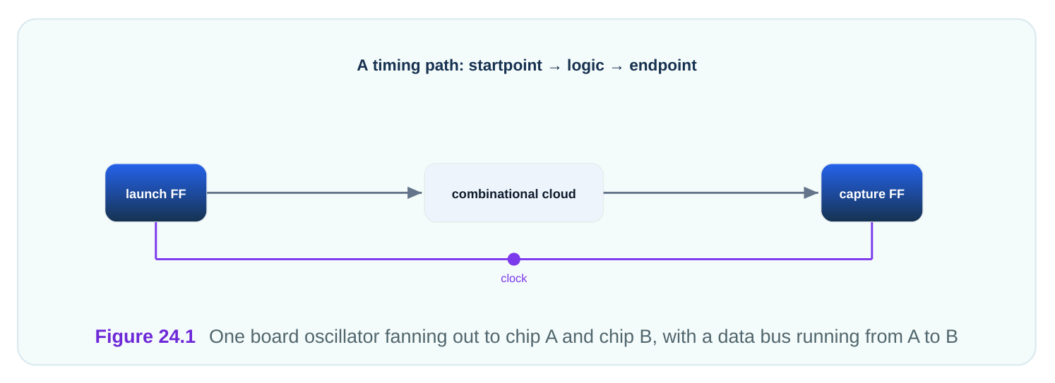
The phrase common-clock is often used for the same idea. Both endpoints share a common clock. We treat the two phrases as the same thing here.
Budgeting the Path: Where the Period Goes
Think of one clock period as a budget of time. Many things spend from that budget. Whatever is left is your margin. Here is the chain of events for one bit moving from chip A to chip B:
- 1. The system clock edge reaches chip A's launch flip-flop.
- 2. After the flop's clock-to-output delay, data appears on chip A's output pin.
- 3. The data crosses the board wire. This travel time is the flight time.
- 4. The data arrives at chip B's input pin.
- 5. The data must settle before chip B's capture edge, by the setup time.
| Budget item | What it is | Example value |
|---|---|---|
| Clock period | Time between edges | 4.58 ns |
| Chip A clock-to-output | Delay from clock edge to valid output | 1.37 ns |
| Flight time | Board wire travel A to B | 0.62 ns |
| Chip B setup time | Data must be stable before edge | 0.41 ns |
| Remaining margin | What is left over | 2.18 ns |
If the remaining margin is positive, the link works. If it is negative, the link fails setup. Setup failure means data arrives too late to be captured cleanly. The clock itself is not perfectly aligned between the two chips. The two copies of the clock may arrive at slightly different times. This difference is clock skew. Skew also spends from the budget. We fold it into uncertainty later.
Telling the Timing Tool About the Outside World
The timing tool only sees one chip at a time. It does not know what chip A does, when it is timing chip B. So we model the outside world with two commands.
set_input_delay tells chip B how late its input data arrives, relative to the clock edge. The valuebundles chip A's clock-to-output delay plus the flight time.
set_output_delay tells chip A how much time the outside world needs after chip A's output, beforethe capture edge. The value bundles flight time plus chip B's setup time. Both commands hang off a clock. The clock named in the command is the same system clock, defined on the chip's clock port.
# standard SDC — portable across compliant tools
create_clock -name sys_clk -period 4.58 [get_ports clk_in]
# input delay seen by the receiving chip, on its data bus
set_input_delay -clock sys_clk -max 1.99 [get_ports {data_in[*]}]
set_input_delay -clock sys_clk -min 0.73 [get_ports {data_in[*]}]
The -max value is the worst late case. It drives the setup check. The -min value is the worst early case. It drives the hold check. Hold means data must not change too soon after the edge, or the new value races ahead and corrupts the captured bit. Here is the output side, written from chip A's view:
# standard SDC — portable across compliant tools
create_clock -name sys_clk -period 4.58 [get_ports clk_in]
# output delay: time the board + receiver need after chip A drives
set_output_delay -clock sys_clk -max 1.03 [get_ports {data_out[*]}]
set_output_delay -clock sys_clk -min 0.28 [get_ports {data_out[*]}]
The -max output delay holds flight time plus the far chip's setup. The -min output delay can go negative when the far chip's hold need is small and flight time is large.
A Worked Budget for Setup and Hold
Let us walk one full setup check from chip B's view. Chip B is the receiver. Its capture flip-flop must see stable data before the edge.
# Worked illustrative example — setup check at chip B
Clock period                         = 4.58 ns
Input delay (-max)                   = 1.99 ns   (data arrives this late)
Internal path to capture flop        = 0.34 ns   (inside chip B)
Capture flop setup time              = 0.41 ns
Time data is ready at capture flop   = 1.99 + 0.34       = 2.33 ns
Time the edge needs data by          = 4.58 - 0.41       = 4.17 ns
Setup slack                          = 4.17 - 2.33       = 1.84 ns
Slack is the leftover time. Positive slack of 1.84 ns means setup passes with room to spare. Now the hold check. Hold cares about the early case. It uses the -min input delay.
# Worked illustrative example — hold check at chip B
Input delay (-min)                   = 0.73 ns   (data arrives this early)
Internal path to capture flop        = 0.34 ns
Capture flop hold time               = 0.16 ns
Earliest data change at capture flop = 0.73 + 0.34       = 1.07 ns
Edge needs data held until           = 0.00 + 0.16       = 0.16 ns
Hold slack                           = 1.07 - 0.16       = 0.91 ns
Positive hold slack of 0.91 ns means the early data still arrives after the hold window closes. Both checks pass, so this bit is safe.
Flight Time and How to Budget It
Flight time is the travel time of a signal down a board wire. Copper is not instant. A signal moves at a fraction of the speed of light through a board, often around 6 inches per nanosecond. So a 4-inch trace adds roughly 0.67 ns of flight time. A short 1-inch trace adds about 0.17 ns. The timing tool does not know the board. You must put flight time into the delay numbers by hand or from a board model.
| Trace length | Approx flight time | Notes |
|---|---|---|
| 1.0 inch | 0.17 ns | short, on-package style |
| 4.0 inch | 0.67 ns | typical board hop |
| 7.5 inch | 1.26 ns | long, across a board |
A common mistake is to forget flight time entirely. Then the set_input_delay value is too small. The tool reports false good slack. The board then fails in the lab. Always include the wire. Notice a tension. Longer wires help hold but hurt setup. A long wire delays the data. Late data is bad for setup but good for hold, because hold wants the data to stay put past the edge. Board designers balance the two.
Contrast with Source-Synchronous
The system-synchronous style ties speed to flight time. The whole budget is one clock period, and skew between the two clock copies eats into it. As frequencies climb past a few hundred MHz, skew becomes a big share of the budget. The link runs out of room. The source-synchronous style fixes this. The sender ships a clock alongside the data. The clock and data travel together on matched wires. Because they travel together, flight time mostly cancels out. The receiver uses the forwarded clock to capture the data.
| Feature | System-synchronous | Source-synchronous |
|---|---|---|
| Clock source | One shared board clock | Clock forwarded with data |
| Flight time effect | Eats the budget | Mostly cancels |
| Max practical speed | Lower | Higher |
| Constraint anchor | Shared create_clock | A create_clock on the forwarded clock pin |
| Skew sensitivity | High | Low |
In SDC terms, the source-synchronous receiver defines a clock on the incoming forwarded clock pin. Then it sets input delay relative to that clock, not to the board clock.
# standard SDC — portable across compliant tools
# source-synchronous: clock arrives on its own pin
create_clock -name fwd_clk -period 2.27 [get_ports clk_fwd_in]
set_input_delay -clock fwd_clk -max 0.48 [get_ports {ss_data[*]}]
set_input_delay -clock fwd_clk -min 0.09 [get_ports {ss_data[*]}]
Choosing between the two styles is a system decision. System-synchronous is simpler to wire and reason about. Source-synchronous wins when speed matters more than simplicity.
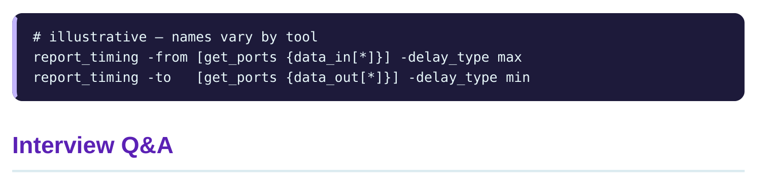
After you write the constraints, you ask the tool to report timing. The exact report names vary.
System-synchronous means both chips run off one shared board clock. The sender launches data on an edge of that clock; the receiver captures on the next edge. "Common-clock" is just another name for the same setup. They are treated as identical. The defining trait is a single oscillator feeding both endpoints, for example a 218.4 MHz source giving a 4.58 ns period.
receiver? You bundle the sender's clock-to-output delay and the board flight time. For example, 1.37 ns clock-to-output plus 0.62 ns flight time gives a 1.99 ns input delay. That single number tells the tool how late the data shows up at the receiver's pin, measured from the shared clock edge.
case and drives the setup check, where data must arrive in time. The -min value models the worst early case and drives the hold check, where data must not change too soon. If you supply only -max , the tool may report a bogus hold result. With a -max of 1.99 ns and a -min of 0.73 ns, the tool checks both ends of the arrival window.
hurts setup, because the data may miss its capture edge. But late data helps hold, because the data stays valid past the edge, which is what hold wants. A 1.26 ns flight time on a 7.5-inch trace is a big setup cost but a hold benefit. Board designers tune trace length to balance both.
synchronous, the whole budget is one clock period and the skew between the two clock copies eats a growing share as frequency rises. In source-synchronous, the clock travels with the data on matched
wires, so flight time and much of the skew cancel. That lets the link run at, say, a 2.27 ns period where a shared-clock link would fail.
Data arrives at 1.99 ns input delay, plus 0.34 ns internal path, so it is ready at 2.33 ns. The edge needs it by period minus setup, 4.58 minus 0.41, which is 4.17 ns. Slack is 4.17 minus 2.33, equal to 1.84 ns. Positive slack means setup passes.
Key Takeaways
- System-synchronous (common-clock) links share one board clock; the budget for one bit is roughly one clock period minus all losses.
set_input_delaybundles the sender's clock-to-output plus flight time;set_output_delaybundles flight time plus the far chip's setup time.- Always supply
-maxand-minso the tool can check setup with the late case and hold with the early case. - Flight time must be added by hand because the tool cannot see the board; longer wires hurt setup but help hold.
- Source-synchronous forwards the clock with the data so flight time cancels, which is why it scales to higher speeds than common-clock.
Comments
Leave a Reply