 ChipBuddy
← Home
ChipBuddy
← Home
Driving Cell & Load Modeling
Driving Cell & Load Modeling (Deep)
A chip's pins do not float in space. Every input pin is driven by something on the outside. Every output pin must charge something on the outside. The timing tool cannot see those outside things. So you must describe them. You describe the driver of an input and the load on an output. This chapter goes deep on how those descriptions shape the slews and delays that the tool computes. We keep the format generic. We call it SDC. We never name a tool or a company. We say "the timing tool" for the engine that checks paths and "the synthesis tool" for the engine that builds logic.
Why a Driver Description Matters
When a signal enters your chip, its shape is not perfect. It has a slope. The slope is called transition or slew. Slew is the time a signal takes to swing from low to high or high to low. A sharp slew is fast. A lazy slew is slow. The slew at an input pin depends on what is driving it outside. A strong driver makes a sharp slew. A weak driver makes a lazy slew. The first gate inside your chip then inherits that slew. Its own delay depends on the incoming slew. A lazy input slew makes the first gate slower. So the outside driver reaches into your timing. If you tell the tool nothing, it assumes a perfect, instant slew at the input. That is too optimistic. The first gate looks faster than it really is. Setup slack looks better than the truth. You ship a chip that fails. So you must model the driver.
Two Ways to Model an Input Driver
There are two common ways. The first describes the actual driving gate. The second describes only the resulting slew. The command set_driving_cell names a library cell that stands in for the external driver. The tool then computes the slew the way it would for that real cell, accounting for the load it sees. This is the rich, realistic choice. It reacts to load and corner like a real gate. The command set_input_transition skips the gate and states the slew directly. You simply tell the tool the rise and fall slew at the pin. This is the simple, blunt choice. It does not react to anything. It is a fixed number.
| Approach | What you give | Reacts to load? | When to use |
|---|---|---|---|
| set_driving_cell | A library cell name | Yes | Realistic boundary, known driver type |
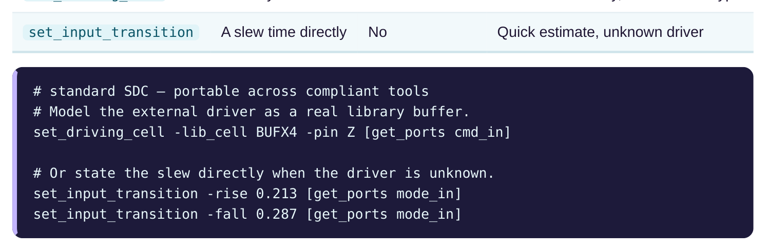
A worked feel. Suppose set_driving_cell for cmd_in makes the tool compute an input slew of 0.341 ns. The first inverter inside, fed that slew, computes a delay of 0.094 ns. Now switch to a perfect-slew assumption. The same inverter computes 0.061 ns. The driver model added 0.033 ns to that one stage. Across a long path, such differences pile up and decide pass or fail.
Modeling the Output Load
An output pin must charge the wires and gates of the outside world. That charge is capacitance. Capacitance is the electrical "size" of what the pin must drive. A big load is slow to charge. A small load is fast. The command set_load states the capacitance the output pin must drive. A larger value makes the last gate inside your chip slower, because it works harder to swing the load. If you state nothing, the tool assumes a tiny or zero load. The output looks far faster than reality. Load has two parts. There is pin capacitance, the input capacitance of the gates outside. There is wire capacitance, the capacitance of the metal route between your pin and those gates. A careful model adds both. A rough model lumps them into one number.
| Load component | What it is | Typical source |
|---|---|---|
| Pin capacitance | Input cap of external gates | Sum of fanout gate inputs |
| Wire capacitance | Cap of the external metal route | Estimated from route length |
| Total load | Sum of the above | What set_load should carry |
# standard SDC — portable across compliant tools
# Total external load: external pins plus the board/route wire.
set_load 0.0472 [get_ports data_out]
# Some flows let you tag the wire portion explicitly.
set_load -wire 0.0190 [get_ports addr_out]
External Fanout and Why It Changes Slew
Fanout is the number of gate inputs a signal must drive. More fanout means more total capacitance. More capacitance means a slower, lazier slew at the output and a longer last-stage delay. Outside your chip, fanout still exists. An output pin may feed three external chips. Each adds input capacitance. If you model only one, the tool underestimates the load and overestimates speed. Some flows let you express the external fanout count so the tool can reason about drive strength and slew degradation at the boundary.
A worked feel. An output drives a wire plus two external inputs. Each input is 0.0121 pF. The wire is 0.0205 pF. Total load is 0.0447 pF. With this load the last buffer computes a slew of 0.398 ns. Drop to one external input and the wire, and the load falls to 0.0326 pF, and the slew tightens to 0.331 ns. The fanout you declare directly moves the slew.
Putting Driver and Load Together
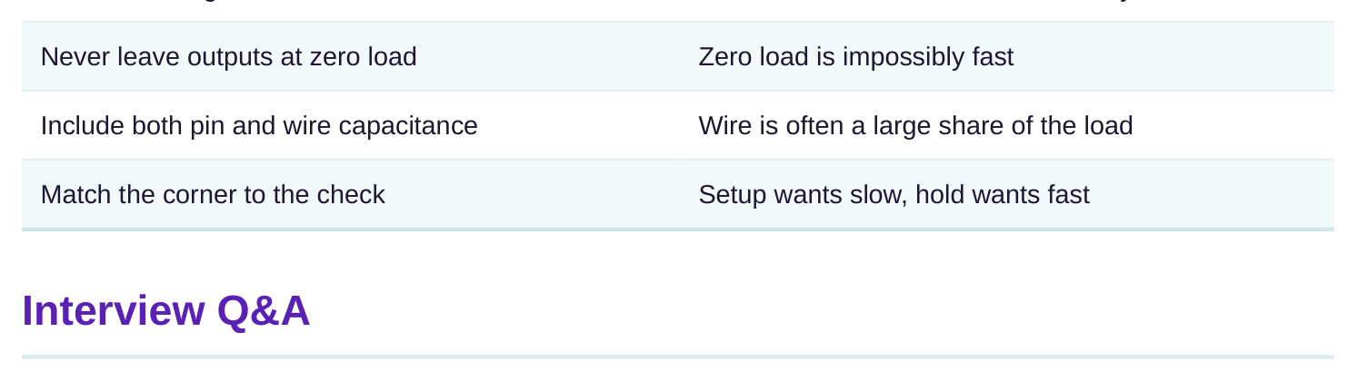
A realistic boundary models both sides. Inputs get a driver. Outputs get a load. Together they turn the idealized boundary into something that behaves like the real board. The payoff is honest slack. The cost is a little more setup work. There is a corner subtlety. Setup checks want the worst, slowest behavior. Hold checks want the fastest. A driver model and a load model both shift with corner. A strong driver and small load make hold worse, because signals race. A weak driver and large load make setup worse, because signals crawl. Good boundary modeling therefore feeds both checks the corner that stresses them.
# standard SDC — portable across compliant tools
# A complete, realistic boundary for one path.
set_driving_cell -lib_cell INVX8 -pin Y [get_ports req_in]
set_load 0.0518 [get_ports ack_out]
Two habits keep this clean. First, prefer set_driving_cell when you know the driver type, because it reacts to your own input load and corner. Fall back to set_input_transition only when the driver is a mystery. Second, always give outputs a non-zero set_load . A zero load is never real and always too optimistic.
| Habit | Why it matters |
|---|---|
| Prefer a driving cell over a fixed slew | It reacts to load and corner like reality |
slew, the slope of the incoming signal. The first internal gate computes its own delay from that incoming slew. A lazy driver slew makes that gate slower, so the outside driver reaches into the chip's internal path delays.
set_driving_cell names a real library cell as the driver, so the tool computes slew the way that cellwould, reacting to the load it sees. set_input_transition simply states a fixed slew number that never reacts to anything. The first is realistic, the second is a blunt estimate.
slew. The first gate looks faster than it really is. Setup slack looks better than the truth, which can hide a real violation and lead to silicon that fails.
the output pin must charge. It has two parts: pin capacitance from the input of external gates, and wire capacitance from the external metal route. A careful model sums both; ignoring either underestimates the load.
more total capacitance. More capacitance makes the last gate work harder, producing a lazier slew and a longer last-stage delay. Underdeclaring fanout makes the output look faster than it is.
large load slow signals down, which stresses setup. A strong driver and small load speed signals up, which stresses hold. Good boundary modeling gives each check the corner that hurts it most.
Key Takeaways
- The boundary is not ideal. Inputs are driven and outputs are loaded, and ignoring either makes timing look falsely optimistic.
- A driving cell reacts; a fixed slew does not. Prefer
set_driving_cellwhen the driver type is known, because it tracks load and corner.
- Load has pin and wire parts. A trustworthy
set_loadsums both, since wire capacitance is often a large share. - Fanout moves slew. More external loads mean more capacitance, lazier slews, and longer last- stage delays.
- Corners cut both ways. Weak-and-heavy stresses setup, strong-and-light stresses hold, so model each side for the check it threatens.
Comments
Leave a Reply