 ChipBuddy
← Home
ChipBuddy
← Home
The MOS Transistor — How It Switches
Every chip you own runs on tiny switches. Billions of them. These switches are MOSFETs (metaloxide-semiconductor field-effect transistors, the basic building block of modern chips). This chapter explains how one MOSFET works. Master this, and the rest of CMOS design follows naturally. We will keep things simple. Think of a transistor as a faucet for electric current. A small signal at one terminal opens or closes the flow. No moving parts. Just voltage doing the work.
What a MOSFET Really Is
A MOSFET is a voltage-controlled switch. You apply a voltage to one terminal. That voltage decides whether current can flow between two other terminals. Every MOSFET has four terminals.
- Gate: the control knob. Voltage here turns the switch on or off.
- Source: where the charge carriers enter.
- Drain: where the charge carriers leave.
- Body: the silicon underneath. Often tied to a fixed voltage.
The gate sits on top of a very thin insulator. This insulator is usually silicon dioxide (a glass-like layer that blocks current). Because of this layer, almost no current flows into the gate. The gate works by its electric field alone. That is the "field-effect" in the name.
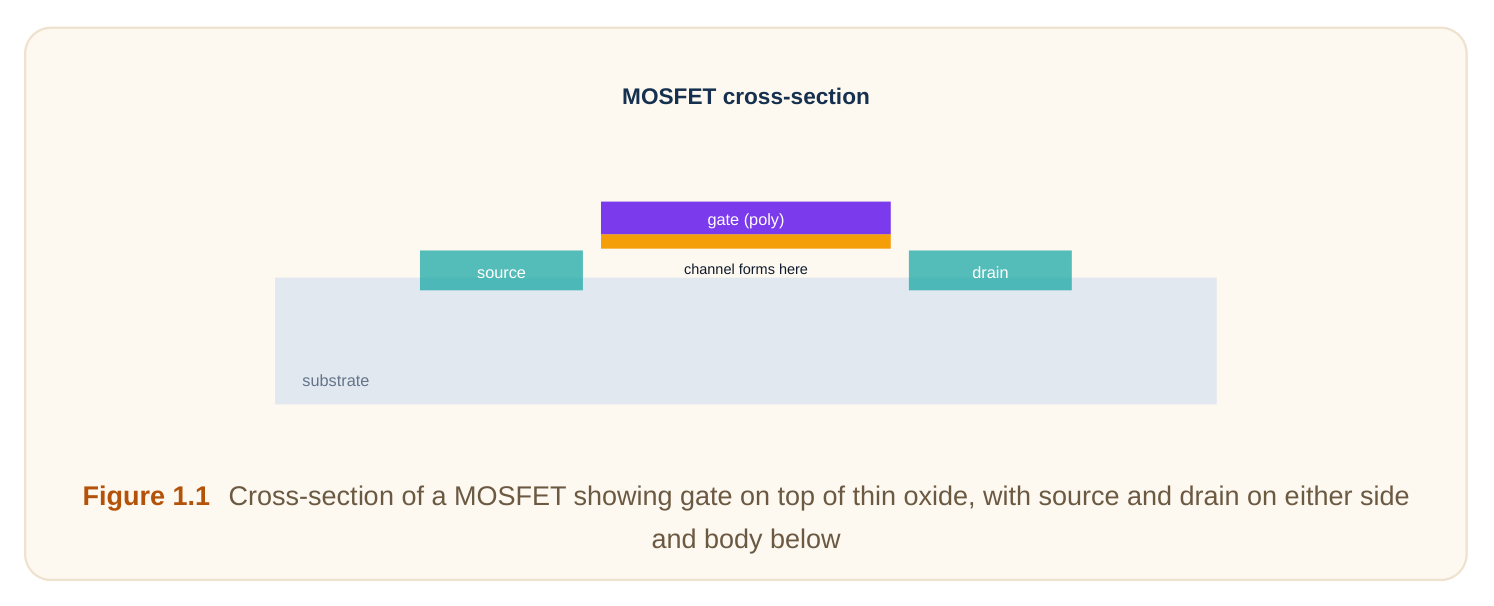
Here is the faucet analogy. The gate is the handle. The source and drain are the two ends of the pipe. The body is the surrounding metal of the faucet. Turn the handle (apply gate voltage) and water (current) flows from one end to the other. There are two flavors of MOSFET. NMOS and PMOS. They are mirror images of each other.
NMOS vs PMOS
An NMOS transistor (n-channel MOSFET) uses electrons to carry current. It turns on when the gate voltage is high. A PMOS transistor (p-channel MOSFET) uses holes to carry current. A hole is just a missing electron that acts like a positive charge. PMOS turns on when the gate voltage is low. Think of NMOS as "active high." It wakes up with a 1. Think of PMOS as "active low." It wakes up with a 0. This opposite behavior is the whole secret of CMOS (complementary MOS, where NMOS and PMOS work as a team). We will see why later in the chapter. Here is a side-by-side comparison.
| Feature | NMOS | PMOS |
|---|---|---|
| Carrier type | Electrons | Holes |
| Source connected to | Lower voltage (often ground) | Higher voltage (often supply) |
| Turns ON when | Gate is HIGH | Gate is LOW |
| Threshold voltage sign | Positive | Negative |
| Speed | Faster | Slower |
| Symbol arrow | Points in | Points out |
NMOS is faster than PMOS. Electrons move more easily than holes. We will return to this when sizing transistors in later chapters. One more habit worth building early. Always identify the source before judging a transistor. The source is the terminal at the lower voltage for NMOS. It is the terminal at the higher voltage for PMOS. Source and drain are physically similar. Which one is which depends on the voltages applied. Getting this right keeps your Vgs calculation correct. NMOS and PMOS symbols
| D | D |
|---|---|
| G | G |
| S | S |
| NMOS | PMOS |
| on when gate HIGH | on when gate LOW |
Figure 1.2 Schematic symbols for NMOS and PMOS side by side, labeled with gate, source, drain
The Threshold Voltage Idea
A MOSFET does not turn on gradually from zero. It needs a minimum push. That minimum push is the threshold voltage (the gate voltage where the transistor just starts to conduct). We write it as Vt. Below Vt, the switch is essentially off. Above Vt, the switch turns on. It is like a door with a stiff hinge. You must push hard enough before it opens at all. Why does the gate control a channel? Let us picture an NMOS device. The body is p-type silicon. It has very few electrons. So no current can flow from source to drain. The pipe is blocked.
Now raise the gate voltage. The positive gate attracts electrons toward the surface. These electrons gather right under the oxide. When enough gather, they form a thin conducting layer. This layer is the channel (a path of charge that lets current flow from source to drain). The gate voltage where the channel just forms is the threshold voltage. Below it, no channel. Above it, a channel exists.
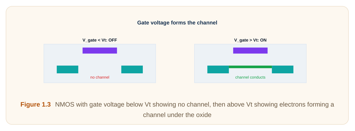
This is called enhancement mode. The device is off by default. You "enhance" it into conduction by applying gate voltage. Almost all digital MOSFETs are enhancement mode. A simple rule helps here. What matters is the gate-to-source voltage, written Vgs. Not the gate voltage alone. For NMOS: the channel forms when Vgs > Vt. The amount by which you exceed the threshold is the overdrive voltage (Vgs minus Vt). More overdrive means a stronger channel and more current. Push the door harder and it swings wider.
Operating Regions in Plain Terms
A MOSFET behaves in three distinct ways. These are called operating regions. The region depends on the gate and drain voltages. Let us walk through each one for an NMOS device.
CUTOFF: THE SWITCH IS OFF
When Vgs < Vt, there is no channel. Almost no current flows. The transistor is off. This is the open switch. The pipe is blocked. We treat current here as effectively zero (though tiny leakage exists, as we will see).
LINEAR / TRIODE: THE SWITCH ACTS LIKE A RESISTOR
When Vgs > Vt and the drain voltage is small, the channel is fully open along its length. Current flows easily.
In this region the transistor behaves like a resistor. A small drain-source voltage produces a proportional current. Double the voltage, roughly double the current. This region is also called the triode region or the linear region. It is how a turned-on transistor pulls an output toward a rail. Qualitatively, current rises with both the overdrive (Vgs − Vt) and the drain-source voltage (Vds). Picture the faucet again. In triode the valve is open and the pipe is short. Push a little more pressure and a little more water flows. The relationship is roughly straight at first. That is why we call it linear. As the drain voltage grows, though, the line starts to bend. The channel near the drain begins to thin out. This bending is the warning sign that saturation is coming next.
SATURATION: THE SWITCH ACTS LIKE A CURRENT SOURCE
When Vgs > Vt but the drain voltage is large, something interesting happens. The channel near the drain gets pinched thin. This is called pinch-off. Now the current stops climbing with more drain voltage. It flattens out. The transistor acts like a current source. It pushes a roughly fixed current regardless of drain voltage. In saturation, current depends mostly on the overdrive squared. So (Vgs − Vt) matters a lot, but Vds barely matters.
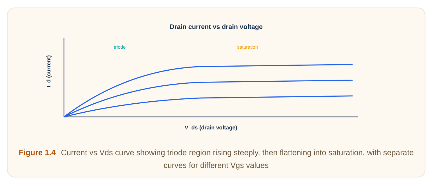
Here is the boundary rule. The transistor is in saturation when Vds > Vgs − Vt. Otherwise, if conducting, it is in triode. This table summarizes all three regions for an NMOS device.
| Region | Condition | Behavior | Current depends on |
|---|---|---|---|
| Cutoff | Vgs < Vt | Off, open switch | Nearly zero |
| Triode (linear) | Vgs > Vt and Vds < Vgs − Vt | Acts like a resistor | Vds and overdrive |
| Saturation | Vgs > Vt and Vds > Vgs − Vt | Acts like a current source | Overdrive squared |
For PMOS, the same ideas hold but the signs flip. The threshold is negative. The device turns on when Vgs is sufficiently negative.
Why NMOS Passes Strong 0 and Weak 1
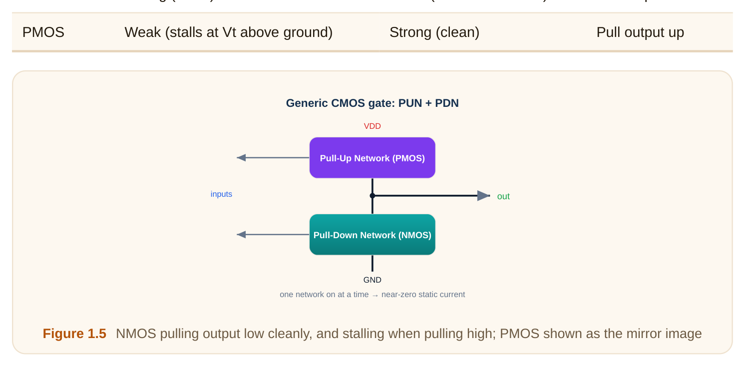
This is one of the most important ideas in CMOS. It explains why we always use NMOS and PMOS together. Imagine an NMOS transistor passing a signal. The gate is held high to keep it on. We want it to pass a logic value to the output. Passing a 0 (strong 0): The source sits near ground. The gate is high. So Vgs stays large. The channel stays strong. The output is pulled all the way down to 0. This is a clean, strong 0. Passing a 1 (weak 1): Now the output rises toward the high voltage. But as the output rises, the source voltage rises too. The gate stays fixed. So Vgs shrinks. When the output reaches one threshold below the supply, Vgs drops to Vt. The transistor shuts itself off. The output never reaches the full high value. It stalls at supply minus Vt. This is a weak 1. So NMOS is great at pulling down but poor at pulling up. PMOS is the mirror image. Passing a 1 (strong 1): PMOS pulls the output all the way up to the supply. Clean and strong. Passing a 0 (weak 0): PMOS cannot pull below one threshold above ground. It gives a weak 0. This is why CMOS pairs them. NMOS pulls outputs down to a clean 0. PMOS pulls outputs up to a clean 1. Together they give full, strong logic levels in both directions. Neither transistor is asked to do the job it is bad at.
| Transistor | Passes 0 | Passes 1 | Best used to |
|---|---|---|---|
| NMOS | Strong (clean) | Weak (stalls at Vdd − Vt) | Pull output down |
Body Effect and Leakage
Two real-world effects matter even in a simple model. Both affect how a transistor switches.
BODY EFFECT
So far we assumed the source and body sit at the same voltage. Often they do not. When the source voltage rises above the body voltage, the threshold voltage increases. Harder to turn on. This is the body effect (the rise in threshold voltage when the source and body differ in voltage). Think of it as the door hinge getting stiffer. You now need more gate voltage to open the channel. The body effect matters in stacked transistors. When transistors sit in series, the upper ones have raised sources. Their thresholds creep up. They become slightly weaker. Designers account for this when sizing.
LEAKAGE AND SUBTHRESHOLD CONDUCTION
Earlier we said cutoff current is "nearly zero." Not exactly zero. A small current still leaks even below threshold. This is subthreshold conduction (the small current that flows when the gate is just below the threshold voltage). The channel is not fully off. A trickle of carriers still crosses. This trickle is small per transistor. But a modern chip has billions of transistors. The leakage adds up. It drains battery even when the chip does nothing. Leakage rises sharply as Vt is lowered. Lower Vt gives faster switching but more leakage. This is a core tradeoff in chip design. Speed versus power. Subthreshold current also grows with temperature. A hot chip leaks more. More leakage makes the chip hotter still. Designers watch this loop carefully. Modern parts often use several threshold voltages on one chip. Fast paths get low-Vt transistors. Idle blocks get high-Vt transistors to save power. Mixing them is a common low-power trick. We will revisit it in later chapters on power.
| Effect | Cause | Consequence |
|---|---|---|
| Body effect | Source voltage above body voltage | Threshold voltage rises, slower switching |
| Subthreshold leakage | Gate just below threshold | Small unwanted current, wastes power |
Worked Example 1: Is the Transistor On or Off?
Let us decide whether an NMOS transistor is on or off. Given values: - Threshold voltage, Vt = 0.4 V - Gate voltage = 1.1 V - Source voltage = 0.2 V Step 1: Find Vgs.
Vgs = gate voltage − source voltage = 1.1 − 0.2 = 0.9 V. Step 2: Compare Vgs to Vt. 0.9 V > 0.4 V. So Vgs exceeds the threshold. Conclusion: The transistor is ON. A channel has formed. Step 3: Find the overdrive voltage. Overdrive = Vgs − Vt = 0.9 − 0.4 = 0.5 V. A 0.5 V overdrive means a healthy, conducting channel. Now suppose the source rose to 0.8 V instead. Then Vgs = 1.1 − 0.8 = 0.3 V. That is below Vt = 0.4 V. The transistor would be OFF. This shows how a rising source can shut an NMOS device down. It is exactly the weak-1 problem from earlier.
Worked Example 2: Which Region Is It In?
Now let us find the operating region of a conducting NMOS transistor. Given values: - Threshold voltage, Vt = 0.5 V - Gate-source voltage, Vgs = 1.2 V - Drain-source voltage, Vds = 0.3 V Step 1: Check if it is on. Vgs = 1.2 V > Vt = 0.5 V. Yes, it is on. So it is either triode or saturation. Step 2: Find the overdrive. Overdrive = Vgs − Vt = 1.2 − 0.5 = 0.7 V. Step 3: Compare Vds to the overdrive. Vds = 0.3 V. Overdrive = 0.7 V. Since 0.3 V < 0.7 V, we have Vds < (Vgs − Vt). Conclusion: The transistor is in the TRIODE region. It acts like a resistor. Now change Vds to 0.9 V. Then Vds = 0.9 V > overdrive 0.7 V. The condition flips. The transistor enters SATURATION. It now behaves like a current source. Same device, different region, just by raising the drain voltage.
Interview Q&A
The gate sits on a thin insulating oxide. This oxide blocks direct current. The gate works only through its electric field. So a MOSFET costs almost no current to hold in a state. This low static gate current is why CMOS is power efficient.
It is the gate-to-source voltage at which a conducting channel just forms. Below it, the device is effectively off. Above it, a channel exists and current can flow. It sets the on-off boundary of the switch.
NMOS conducts using electrons. PMOS conducts using holes. Electrons move more easily through silicon than holes. So for the same size and voltage, NMOS carries more current and switches faster. This is why PMOS devices are often made wider to keep up.
NMOS passes a strong 0 but only a weak 1. Its output stalls one threshold below the supply when pulling high. The logic high would be degraded. We pair it with PMOS, which passes a strong 1. Together they deliver full-swing outputs in both directions.
It is the small current that flows even when the gate is just below threshold. The channel is not perfectly off. Per transistor it is tiny. But across billions of transistors it wastes real power and drains batteries. Managing it is a major concern in low-power design.
Key Takeaways
- A MOSFET is a voltage-controlled switch with four terminals: gate, source, drain, and body.
- The gate controls a channel through an electric field across a thin oxide. It draws almost no current.
- NMOS turns on with a high gate and uses electrons. PMOS turns on with a low gate and uses holes.
- Threshold voltage Vt is the gate-source voltage where the channel just forms. The device is on when Vgs exceeds Vt for NMOS.
- The three regions are cutoff (off), triode (resistor-like), and saturation (current-source-like). The boundary between triode and saturation is Vds versus the overdrive Vgs − Vt.
- NMOS passes a strong 0 and weak 1. PMOS passes a strong 1 and weak 0. This is why CMOS pairs them.
- Body effect raises the threshold when the source sits above the body. Subthreshold leakage wastes power across billions of devices.
- Always work with Vgs, not the gate voltage alone, when deciding if a transistor is on.
Comments
Leave a Reply