 ChipBuddy
← Home
ChipBuddy
← Home
Testing & Design-for-Test
Why Testing Is a Design Problem
A finished chip can still be faulty. A tiny dust speck or a process flaw can break one transistor. You cannot ship broken chips. So every chip is tested after manufacture. But testing a chip with millions of buried flip-flops is hard. You cannot reach inside. So designers add special test circuits during design. This is design-for-test (DFT). This chapter explains the faults, the test idea, and the main DFT methods.
What Can Go Wrong: Fault Models
We cannot test every possible defect. So we use simple fault models. A fault model is a stand-in for real defects. It makes testing measurable.
- Stuck-at fault: a node is stuck at 0 or stuck at 1, no matter what. This is the classic model. It catches many real defects.
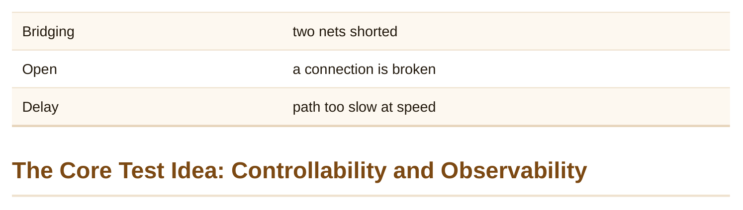
- Bridging fault: two wires that should be separate are shorted together.
- Open fault: a wire that should connect is broken.
- Delay fault: the logic works, but a path is too slow. The chip fails at speed, not at function. Tests are graded by coverage (the fraction of modeled faults a test set can detect). High coverage means few bad chips slip through. Fault model Plain meaning Stuck-at node frozen at 0 or 1
To test a node, you need two things.
- Controllability: can you set that node to a known value from the inputs?
- Observability: can you see that node's value at the outputs? Deep inside a big design, both are hard. A buried flip-flop is far from any pin. DFT exists to fix this. It adds paths to control and observe internal state.
Scan: the Workhorse of DFT
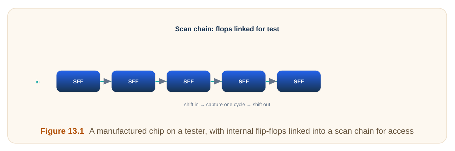
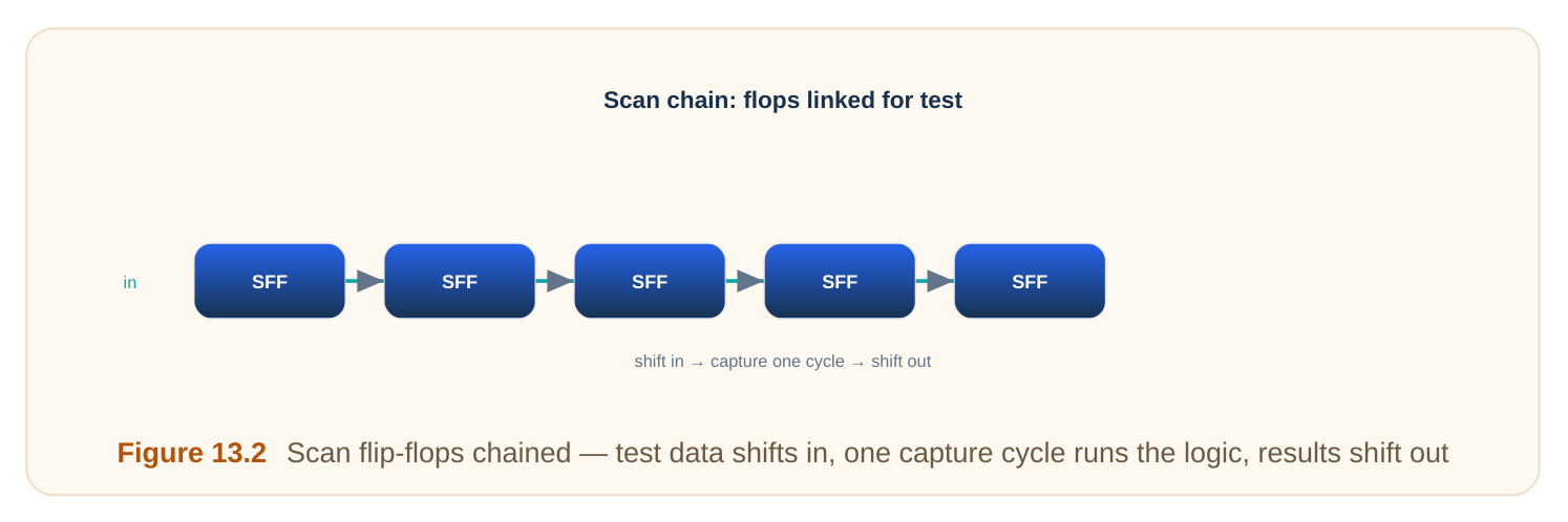
The main DFT method is scan. The idea is simple. Replace normal flip-flops with scan flip-flops. A scan flop has an extra test input and a mode switch. In normal mode, the flop works as usual. In test mode, all the scan flops link into one long shift chain (a scan chain). Now the tester can:
- 1. Shift a known pattern into every flop (full controllability).
- 2. Run one normal clock cycle (let the logic compute).
- 3. Shift the result out and check it (full observability).
This turns an untestable sea of buried flops into a simple shift register the tester can load and read. Scan is the backbone of digital test.
| Scan step | What happens |
|---|---|
| Shift in | load a known pattern into all flops |
| Capture | run one cycle; logic computes |
| Shift out | read results, compare to expected |
Worked example — scan shift time
Suppose a chip has 10,000 scan flops in one chain. Loading a pattern needs 10,000 shift cycles. Reading results needs about 10,000 more. So one test pattern costs roughly 20,000 cycles. With many patterns, this is slow. The fix is to split flops into several shorter chains that shift in parallel. Ten chains of 1,000 flops cut the shift time about tenfold.
Generating the Patterns: ATPG
Who decides the test patterns? A tool called ATPG (automatic test pattern generation). It looks at the netlist and the fault list. For each fault, it computes an input pattern that:
- forces the faulty node to the opposite of its stuck value (to activate the fault), and
- propagates the effect to an observable output (to detect it). ATPG aims for high fault coverage with few patterns. Fewer patterns means cheaper, faster testing. Scan makes ATPG practical, because every flop is controllable and observable.
Built-In Self-Test (BIST)
Sometimes the chip tests itself. This is BIST (built-in self-test). The chip includes a pattern generator and a result checker on-chip. It runs a test without a big external tester.
- Logic BIST: generates pseudo-random patterns and compresses the responses into a signature. A wrong signature means a fault.
- Memory BIST: a small engine writes and reads memory patterns to find memory faults. Memories are dense and regular, so a dedicated engine is efficient. BIST is great for memories and for in-field testing. It cuts reliance on costly testers. The cost is extra on-chip area. Method Where the test lives Best for Scan + ATPG external tester random logic Logic BIST on-chip self-test, in-field Memory BIST on-chip dense memories
Test Compression and Boundary Scan
Two more ideas come up often.
- Test compression: even with scan, pattern data is huge. Compression sends compact data to the chip, expands it into many scan chains, and compresses the responses back. This slashes test time and tester memory.
- Boundary scan: special cells at the chip's pins form a scan ring around the edge. This lets a tester check the connections between chips on a board, not just inside one chip. It is widely used for board-level test.
At-Speed Testing for Delay Faults
A stuck-at test runs slowly. It catches function faults. But it misses delay faults (a path too slow). To catch those, you test at-speed. You apply two close clock pulses. The logic must produce the right result within one real clock period. If a path is too slow, the at-speed test fails it. This is essential for catching speed defects that a slow test would pass.
Worked example — why at-speed matters
A chip is meant to run at a 1.0 ns period. A defect makes one path take 1.1 ns. A slow stuck-at test gives the path plenty of time, so it passes. The chip looks good but fails in a real system. An at-speed test enforces the 1.0 ns window. It catches the slow path and rejects the bad chip.
Interview Q&A
regardless of inputs. It is simple, easy to target with patterns, and catches a large share of real defects. High stuck-at coverage is a standard quality measure, which is why it is the default fault model.
Scan links all flops into a shift chain in test mode, so the tester can load any pattern into every flop and read every result. It turns an untestable design into a controllable, observable one.
activate the fault (set the node opposite to its stuck value) and propagate its effect to an output. It targets high fault coverage with as few patterns as possible. Scan makes ATPG practical.
on the chip, so it tests itself with little external equipment — ideal for memories and in-field test. Scan+ATPG relies on an external tester applying pre-computed patterns. BIST trades on-chip area for tester independence.
extra time, so they miss delay faults. At-speed testing applies two close clock pulses, forcing the logic to meet the real clock period. This catches paths that are functionally correct but too slow.
Key Takeaways
- Chips must be tested after manufacture; DFT adds circuits so internal nodes become controllable and observable.
- Fault models (stuck-at, bridging, open, delay) make testing measurable; coverage grades a test set.
- Scan chains all flops into a shift register: shift in a pattern, capture one cycle, shift out results — the backbone of test.
- ATPG auto-generates patterns for high coverage; BIST lets the chip test itself (great for memories and in-field).
- At-speed testing catches delay faults that slow stuck-at tests miss; compression and boundary scan extend test efficiency and reach.
Comments
Leave a Reply