 ChipBuddy
← Home
ChipBuddy
← Home
Yield, Defects & Test — Deep Dive
What Yield and Test Are About
When chips are made, not all of them work. Tiny flaws in manufacturing ruin some dies. Yield is the fraction of dies on a wafer that work correctly. If a wafer holds 500 dies and 400 of them pass, the yield is 80%. Test is the process of checking each chip to see if it works. A bad chip that ships to a customer can cause a product failure, so test must catch defects before chips leave the factory. Good test also helps engineers learn where defects come from, which improves yield over time. This chapter covers defects, yield models, fault models, and the methods used to test chips: scan chains, automatic test pattern generation, built-in self-test, and burn-in. These topics come up often in interviews because they connect physical manufacturing to logical design.
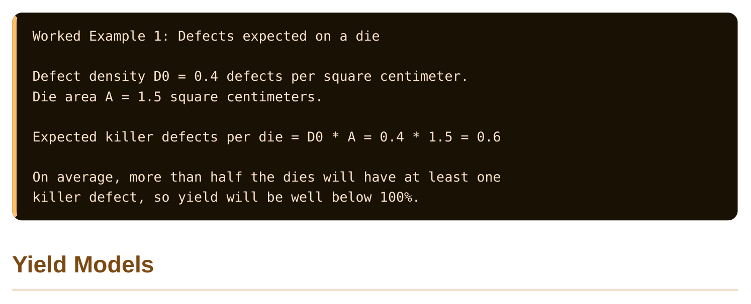
A defect is a physical flaw on the chip. Common defects include a speck of dust that blocks a layer, a metal line that breaks open, two wires shorted together, or a missing connection. Defects can come from particles, chemical problems, or mask errors. Not every defect kills a chip. A defect in empty space does nothing. A defect that lands on a wire or transistor can cause a failure. The chance that a defect causes a failure depends on how much of the chip area is sensitive. Larger chips have more sensitive area, so they catch more defects and have lower yield. The key measure is defect density, written as D0. It is the average number of killer defects per unit area, often per square centimeter. A mature process might have a low defect density, while a new process has a high one.
A yield model is a formula that predicts yield from defect density and die area. The simplest model is the Poisson model. It assumes defects are spread randomly and evenly. The Poisson yield is Y = e^(−D0 × A). This works when defects are truly random. But real defects often cluster together. When defects cluster, fewer dies are hit than the Poisson model predicts, so real yield is higher than Poisson suggests. To handle clustering, engineers use the negative binomial model. It adds a clustering parameter, called alpha. A small alpha means heavy clustering. A large alpha makes the model behave like Poisson. The table compares common models.
| Model | Formula | When to use |
|---|---|---|
| Poisson | Y = e^(−D0·A) | Random, even defects |
| Negative binomial | Y = (1 + D0·A/alpha)^(−alpha) | Clustered defects |
| Murphy | Y = ((1−e^(−D0·A))/(D0·A))^2 | Mixed distributions |
Worked Example 2: Poisson vs negative binomial yield
D0 = 0.4 /cm^2, A = 1.5 cm^2, so D0*A = 0.6
Clustering parameter alpha = 2.
Poisson:
Y = e^(-0.6) = 0.549 = 54.9%
Negative binomial:
Y = (1 + 0.6/2)^(-2) = (1.3)^(-2) = 1/1.69 = 0.592 = 59.2%
Clustering raises predicted yield from 54.9% to 59.2%.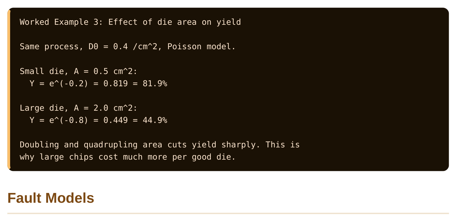
A fault model is a simplified way to describe how a defect changes circuit behavior. We cannot test for every possible physical flaw, so we map flaws onto a few logical fault types. Then we test for those faults. The most common is the stuck-at fault. It assumes a wire is stuck at logic 0 or logic 1, no matter what the circuit tries to drive. A "stuck-at-0" node always reads 0. A "stuck-at-1" node always reads 1. Stuckat faults model broken wires and shorts to power or ground. A bridging fault assumes two wires are accidentally shorted together. When they fight, the result depends on which signal wins. Bridging faults model metal shorts and are harder to test than stuck-at faults. A transition fault, also called a delay fault, assumes a node still reaches the right value but does so too slowly. The logic is correct but the timing is wrong. These faults model weak transistors and resistive connections, and they need at-speed testing to catch.
| Fault model | What it assumes | Models which defects |
|---|---|---|
| Stuck-at | Node fixed at 0 or 1 | Open wires, supply shorts |
| Bridging | Two nodes shorted | Metal shorts between wires |
| Transition | Node switches too slowly | Weak devices, resistive paths |
Scan Chains and ATPG
Testing logic deep inside a chip is hard because we cannot reach internal nodes from the pins. Scan design solves this. In scan design, the normal flip-flops are replaced with scan flip-flops. A scan flipflop can work in two modes. In normal mode it does its real job. In scan mode it links to its neighbors to form a long shift register called a scan chain. In scan mode, test data is shifted into all the flip-flops through one input pin. Then the chip runs one clock cycle in normal mode to capture results. Then the captured values are shifted out through one output pin and compared to expected values. This gives full control and observation of every flip-flop.
ATPG stands for automatic test pattern generation. It is a tool that creates the test patterns. The tool picks each fault from the fault list, then computes the input values that would make the fault show a wrong output. It then merges patterns so that one pattern can catch many faults at once.
Built-in self-test, or BIST, puts the test machinery inside the chip itself. A BIST block generates test patterns on-chip and checks the results on-chip. The chip can then test itself with little outside help. Memory BIST is very common, because large memories need many repetitive patterns that are easy to generate on-chip. The benefit of BIST is that it runs at full chip speed and needs only a simple external tester. The cost is the extra area for the BIST logic. For memories, this cost is small compared to the value of fast, thorough testing. Burn-in is a different idea. It is a stress step where chips run hot and at high voltage for hours. The goal is to force weak chips to fail early, before they ship. Many defects that would fail in the first weeks of use show up during burn-in instead. This catches "infant mortality" failures.
Test coverage measures how good a test is. It is the fraction of modeled faults that the test can detect. If a chip has 100,000 modeled faults and the test catches 99,000 of them, the coverage is 99%. Higher coverage means fewer bad chips slip through.
| Term | Meaning | Why it matters |
|---|---|---|
| BIST | On-chip self-test logic | Fast, simple external test |
| Burn-in | Stress at heat and voltage | Removes early-life failures |
| Test coverage | Percent of faults detected | Predicts escaped defects |
| Defect level | Bad parts shipped per million | Customer-visible quality |
Coverage connects directly to quality. A small gap in coverage can let a few bad chips escape per million shipped. For safety-critical products, teams push coverage very high and add extra fault models.
Interview Q&A
Larger dies have more sensitive area, so they are more likely to be hit by a killer defect. Since the chance of being defect-free falls with area, yield drops as die size grows.
Poisson model assumes defects are random and evenly spread. The negative binomial model adds a clustering parameter, which accounts for defects bunching together. Because clustering hits fewer dies, the negative binomial model predicts higher yield when defects cluster.
of the intended value. This captures broken wires and shorts to power or ground. It is the most common fault model because it is simple and catches many real defects.
data is shifted in, one clock captures results, then results are shifted out and compared. This gives full control and observation of internal flip-flops that pins cannot reach directly.
that takes a fault list and computes input patterns that make each fault produce a wrong output. It also merges patterns so one pattern catches many faults, reducing test time.
but some weak chips pass test yet fail soon in the field. Burn-in stresses chips with heat and voltage to force these weak parts to fail early, removing infant-mortality failures before shipment.
Key Takeaways
- Yield is the fraction of working dies and falls as die area and defect density rise.
- Yield models like Poisson and negative binomial predict yield, with clustering raising the prediction above Poisson.
- Fault models such as stuck-at, bridging, and transition map physical defects onto testable logical behavior.
- Scan chains and ATPG give full control and observation of internal logic and generate efficient test patterns.
- BIST, burn-in, and test coverage together raise quality by testing on-chip, removing early failures, and measuring how many faults are caught.
Comments
Leave a Reply