 ChipBuddy
← Home
ChipBuddy
← Home
Design Flow — RTL to GDSII
What the Design Flow Is
A modern chip is too complex to draw by hand. Instead, designers follow a step-by-step process that turns an idea into a finished chip layout. This process is called the design flow. It is often named "RTL to GDSII," because it starts with RTL and ends with a file called GDSII. RTL stands for register-transfer level. It is a description of the chip's behavior written in a hardware description language. GDSII is the file format that describes the exact shapes of every layer of the chip, which the factory uses to build masks. Each stage of the flow takes an input, transforms it, and produces an output for the next stage. Along the way, the team checks timing, power, and area many times. This chapter walks through each stage, what it produces, and where the key checks happen.
The flow begins with a specification, or spec. The spec is a document that says what the chip must do. It lists the functions, the speed targets, the power budget, the interfaces, and the cost goals. Everything downstream is judged against the spec. Next comes architecture. Architects decide how to split the chip into blocks, how data moves between them, and how fast the clock must run. They make trade-offs between speed, power, and area. The output is a block diagram and a set of rules each block must follow. Then engineers write the RTL. RTL describes the logic as registers (storage elements) and the logic between them. It says what happens on each clock edge. RTL is written in a hardware description language and is checked by simulation, which runs test cases to confirm the logic behaves as the spec demands.
| Stage | Input | Output | Main check |
|---|---|---|---|
| Spec | Idea, requirements | Requirements document | Review by team |
| Architecture | Spec | Block diagram, budgets | Performance modeling |
| RTL | Architecture | RTL code | Functional simulation |
Verification runs alongside RTL. Verification is the effort to prove the RTL is correct. It uses many test cases, random stimulus, and coverage tracking to find bugs early. Finding a bug here is far cheaper than finding it after tape-out.
Synthesis
Synthesis turns RTL into a gate-level netlist. A netlist is a list of standard cells (pre-built logic blocks like gates and flip-flops) and the wires that connect them. The synthesis tool reads the RTL, applies the timing goals, and picks cells from a library to build the logic. Synthesis is where timing first meets real cells. The tool knows each cell's delay and tries to meet the clock speed. It can use faster, larger cells where timing is tight, and smaller, lower-power cells where timing is loose. This is the first real area and power estimate. The tool works against constraints. Constraints tell the tool the clock period, the input and output timing, and which paths are special. These constraints are written in a timing constraint file that follows the design through the whole flow.
Worked Example 1: Picking a cell to meet timing
Clock period = 1.0 nanosecond (1 GHz).
A path has combinational logic plus setup time.
Using small cells:
Logic delay = 0.75 ns, setup = 0.10 ns, total = 0.85 ns
Slack = 1.0 - 0.85 = +0.15 ns. Path passes with margin.
The tool may swap in smaller, lower-power cells to save power
while keeping slack positive. It targets slack near zero.
After synthesis, the team runs gate-level checks. They confirm the netlist still matches the RTL using equivalence checking, a method that proves two descriptions behave the same. They also get a first look at timing and power.
Floorplan and Placement
Floorplanning decides the overall layout. The floorplan sets the chip size, places the big blocks, fixes where the input and output pins go, and reserves space for power and clock routing. A good floorplan makes everything later easier. A bad one causes congestion and timing pain. The power distribution network is built during floorplan. This is the grid of wide metal that carries power and ground across the chip. Designers also place the input and output cells and any large memories at this stage. Placement comes next. Placement decides the exact location of every standard cell. The place-androute tool spreads cells out to balance three goals: short wires, low congestion, and good timing. Cells on a tight timing path are placed close together so their connecting wires are short.
| Stage | Decides | Key output |
|---|---|---|
| Floorplan | Chip size, block locations, power grid | Floorplan database |
After placement, the tool builds the clock tree. The clock signal must reach every flip-flop. But the flipflops are spread across the chip, and the clock must arrive at all of them at nearly the same time. The difference in arrival times is called clock skew. High skew breaks timing. Clock tree synthesis, or CTS, builds a balanced tree of buffers that delivers the clock with low skew. It adds buffer cells along the way to keep the signal strong and the timing even. CTS also tries to keep clock power low, since the clock switches every cycle and burns a lot of power.
Worked Example 3: How skew eats timing margin
Clock period = 1.0 ns.
Logic path delay + setup = 0.90 ns, so raw slack = 0.10 ns.
If clock skew adds 0.08 ns of uncertainty against this path:
Effective slack = 0.10 - 0.08 = 0.02 ns.
The path barely passes. CTS works to keep skew small.
Routing comes after CTS. Routing draws the actual metal wires that connect all the cells and the clock. It uses many metal layers stacked above the transistors. The tool must avoid shorts, meet spacing rules, and still hit timing. Routing is split into global routing, which plans the rough paths, and detailed routing, which draws exact wires.
| Stage | Job | Risk if done poorly |
|---|---|---|
| CTS | Deliver clock with low skew | High skew breaks timing |
| Global routing | Plan wire paths | Congestion |
| Detailed routing | Draw exact metal | Shorts, spacing errors |
Sign-Off and Tape-Out
Sign-off is the final set of checks before the chip is sent to the factory. By now the layout is complete, so the checks use the most accurate models. If sign-off passes, the chip is ready. If not, the team fixes the problems and re-checks. Static timing analysis, or STA, checks that every path meets its timing. STA checks setup time (data must arrive before the clock edge) and hold time (data must stay stable after the clock edge). It checks the worst-case and best-case conditions, since temperature and voltage change the delays. Power analysis confirms the chip stays within its power budget. It adds up switching power and leakage power across the design. Physical verification runs two more checks. Design rule checking, or DRC, confirms the layout obeys the factory's spacing and width rules. Layout-versus-schematic, or LVS, confirms the drawn layout matches the netlist.
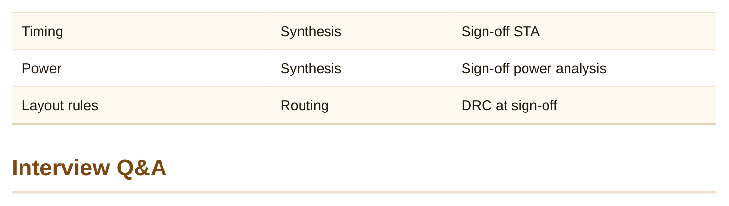
When all checks pass, the team does tape-out. Tape-out is the moment the final GDSII file is sent to the factory to build the masks. After tape-out, the design is locked. The factory makes wafers, the dies are packaged and tested, and the first working chips come back for validation. The table summarizes where each check happens.
| Check | First seen at | Most accurate at |
|---|---|---|
| Functional correctness | RTL simulation | Gate-level simulation |
description of the logic, and ends at GDSII, the file of exact layer shapes the factory uses to make masks. The flow passes through synthesis, placement, clock tree synthesis, routing, and sign-off.
netlist made of standard cells. It is the first stage where real cell delays meet the timing goals, so it gives the first true timing, area, and power estimates against the constraints.
locations, and builds the power grid. A good floorplan keeps wires short and avoids congestion, which makes timing and routing easier. A poor floorplan causes problems that are hard to fix later.
buffers to deliver the clock to every flip-flop at nearly the same time. Skew is the difference in arrival times. High skew eats timing margin and can break setup or hold checks, so CTS aims for low skew.
analysis for the power budget, design rule checking for layout rules, and layout-versus-schematic to confirm the layout matches the netlist. These use the most accurate models.
masks. The design is then locked. It happens only after all sign-off checks pass.
Key Takeaways
- The flow runs from spec and RTL through synthesis, placement, CTS, and routing, ending at GDSII and tape-out.
- Synthesis is the first stage where real cell delays meet timing goals and produces the gate-level netlist.
- Floorplan and placement set locations that keep wires short and control congestion and timing.
- Clock tree synthesis delivers the clock with low skew, which is critical to meeting setup and hold timing.
- Sign-off runs the most accurate timing, power, DRC, and LVS checks before the design is locked at tape-out.
Comments
Leave a Reply