 ChipBuddy
← Home
ChipBuddy
← Home
Memory — SRAM & DRAM
Why Memory Gets Its Own Chapter
Logic computes. Memory remembers. Most chips spend a huge share of their area on memory. So memory design has its own rules and tricks. The goal is to pack many bits into a tiny space. And to read and write them fast and reliably. This chapter covers the two main on-chip memories. They are SRAM and DRAM.
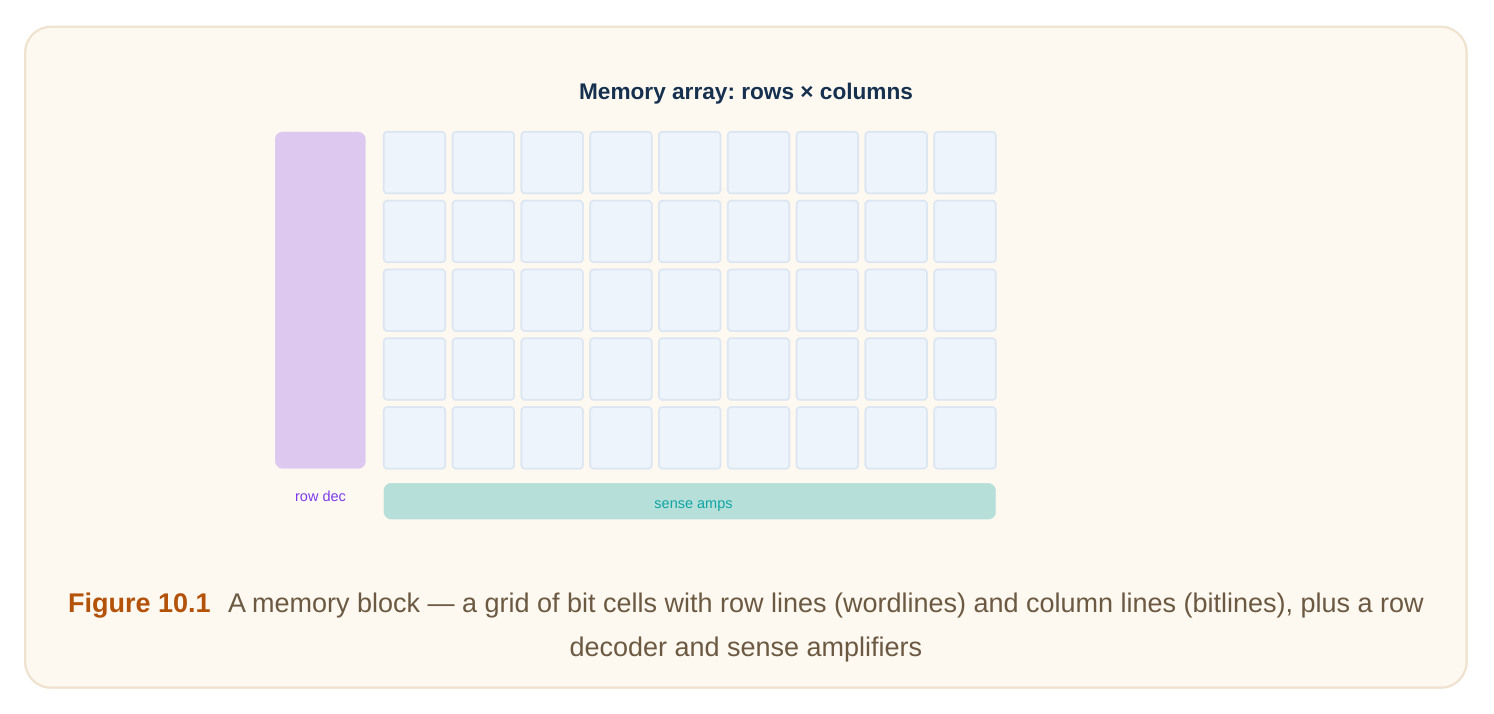
The Memory Array Idea
All memories share one layout idea. Bits sit in a grid. Each bit is a cell (one storage element). The grid has rows and columns.
- A wordline (the row select wire) turns on one whole row.
- A bitline (the column data wire) carries data in or out of each column. To reach one bit, you pick its row and its column. A row decoder (a circuit that turns an address into one active row) raises one wordline. The bitlines then read or write that row. This grid shares wires across many cells. That sharing is what makes memory dense. Part Job Bit cell stores one bit Wordline selects a row Bitline moves data in/out of a column Row decoder address → one active row Sense amplifier reads the tiny bitline signal
SRAM: Fast and Stable
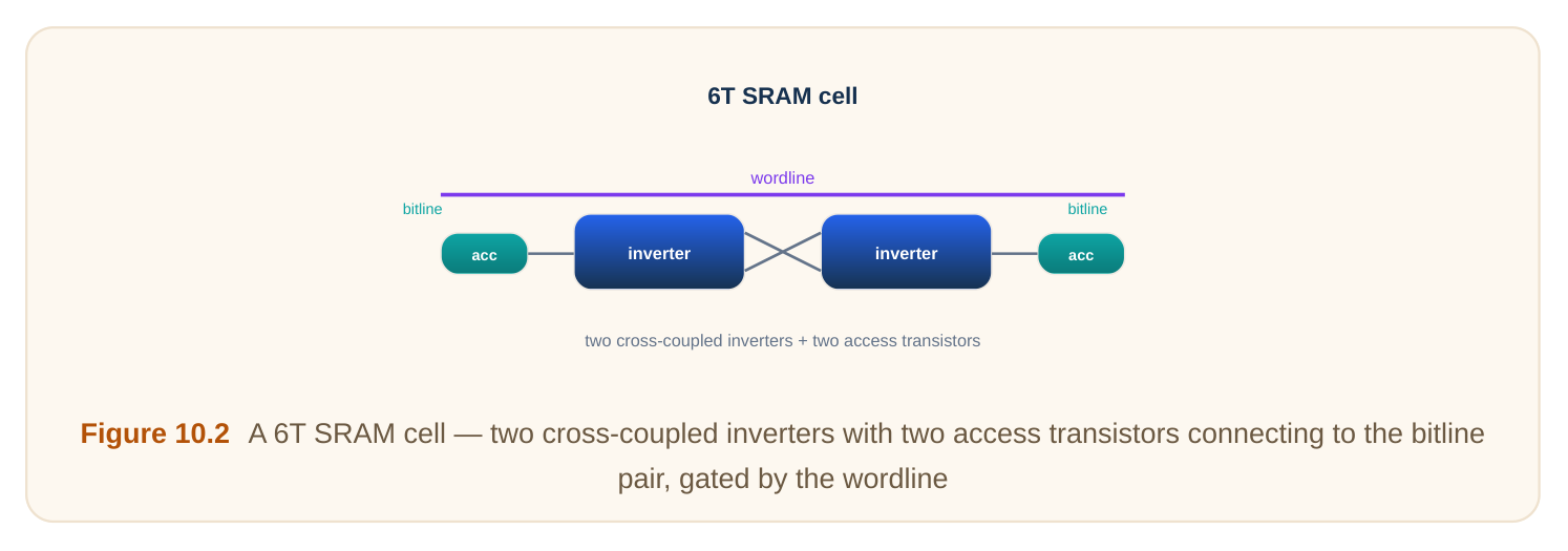
SRAM means static random-access memory. "Static" means it holds its bit as long as power is on. No refresh needed. A classic SRAM cell uses six transistors (called 6T). Two cross-coupled inverters store the bit. Two access transistors connect the cell to the bitlines. The wordline drives those access transistors.
- Read: raise the wordline. The cell gently tips the two bitlines apart. A sense amplifier detects the tiny difference. This gives a fast read.
- Write: raise the wordline. Drive the bitlines hard to the new value. The strong drive flips the cell's loop. SRAM is fast and robust. But six transistors per bit is costly in area. So SRAM is used for caches and registers, where speed matters most. A design tension lives inside the 6T cell. The cell must be easy to write but hard to disturb on read. Transistor sizing balances this. Read stability and write-ability pull in opposite directions.
| SRAM trait | Value |
|---|---|
| Transistors per bit | six (typical 6T) |
| Refresh needed? | no |
| Speed | very fast |
| Density | lower (big cell) |
| Common use | caches, registers |
DRAM: Dense but Leaky
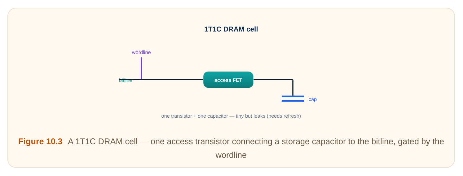
DRAM means dynamic random-access memory. "Dynamic" means it slowly forgets. It must be refreshed often. A DRAM cell uses just one transistor and one capacitor (called 1T1C). The capacitor stores charge. Charge present means one logic value. No charge means the other. The transistor is the access switch, driven by the wordline.
- Read: raise the wordline. The capacitor shares its charge with the bitline. This makes a tiny voltage shift. A sense amplifier detects it. But reading drains the cell, so it must be written back.
- Write: raise the wordline. Drive the bitline. This charges or drains the capacitor. One transistor per bit is tiny. So DRAM is very dense. That is why main memory uses DRAM. The cost is leakage. The capacitor slowly loses charge. So the chip must refresh (re-read and rewrite) every cell on a regular schedule. Refresh costs power and some availability.
| DRAM trait | Value |
|---|---|
| Devices per bit | one transistor + one capacitor |
| Refresh needed? | yes, periodically |
| Speed | slower than SRAM |
| Density | very high (tiny cell) |
| Common use | main memory |
SRAM vs DRAM at a Glance
The two trade speed against density. SRAM is fast but big. DRAM is dense but slow and needs refresh. This is why a system uses both. Fast SRAM caches sit near the processor. Large DRAM holds the bulk of data.
| Feature | SRAM | DRAM |
|---|---|---|
| Cell size | large (6T) | tiny (1T1C) |
| Speed | very fast | slower |
| Refresh | none | required |
| Cost per bit | higher | lower |
| Typical role | cache/registers | main memory |
Worked example — array area
Suppose one bit cell takes area A. A 6T SRAM cell is large. A 1T1C DRAM cell is small, say about one-sixth the area for a rough comparison. For one million bits:
- SRAM array core ≈ 1,000,000 × A.
- DRAM array core ≈ 1,000,000 × (A/6) ≈ 167,000 × A. So DRAM packs the same bit count into roughly one-sixth the cell area. That huge density gap is why bulk memory is DRAM, not SRAM.
Reading Tiny Signals: the Sense Amplifier
Both memories share a problem. A single small cell can only nudge a long, heavy bitline. The resulting voltage change is tiny. A sense amplifier (a circuit that amplifies a small voltage difference into a full logic level) solves this. It often compares the bitline to a reference. It then swings the output to a clean 0 or 1. Good sensing makes memory both fast and reliable. Poor sensing causes read errors. This is why sense-amplifier design is a craft of its own.
Worked example — bitline swing
A DRAM read might shift a bitline by only about 0.05 V. A full logic level might be 0.9 V. The sense amplifier must turn that 0.05 V hint into a clean 0.9 V output. That is nearly a 18× amplification. It must also do this fast and without false reads.
Other Memory Types (Brief)
Beyond SRAM and DRAM, a few others appear in interviews.
- ROM (read-only memory): holds fixed data. The bit pattern is built into the array.
- Flash / non-volatile memory: keeps data with power off. It stores charge on a special floating gate.
- Register file: a small, very fast SRAM-like array with several read/write ports.
- Content-addressable memory (CAM): searches by data, not address. Used in lookups. Memory Volatile? Note SRAM yes fast cache DRAM yes dense main memory ROM no fixed contents Flash no charge on floating gate
Interview Q&A
coupled inverters plus access transistors). It is fast and needs no refresh, but is large. DRAM stores a bit as charge on one capacitor with one access transistor. It is tiny and dense, but slow and must be refreshed because the charge leaks away.
capacitor, which slowly leaks. So the bit must be re-read and rewritten periodically. SRAM holds its bit in a powered feedback loop (cross-coupled inverters), which actively maintains the value as long as power is on.
amount. The resulting signal is far below a full logic level. A sense amplifier amplifies that small difference into a clean 0 or 1, quickly and reliably, enabling fast and correct reads.
disturb during a read. Strong access transistors help writing but can corrupt the stored value on read; weak ones protect reads but hurt writes. Careful transistor sizing balances write-ability against read stability.
fast but uses a big cell, so it suits small, speed-critical caches and registers near the processor. DRAM is slow but its tiny cell gives huge density, so it suits large main memory. Using both gives speed where needed and capacity where needed.
Key Takeaways
- All memories are a grid of cells with wordlines (row select) and bitlines (column data), read by sense amplifiers.
- SRAM is a 6T cell: fast, stable, no refresh, but large — used for caches and registers.
- DRAM is a 1T1C cell: tiny and dense, but slow and needs refresh because charge leaks — used for main memory.
- A sense amplifier turns a tiny bitline change into a full logic level; it is central to speed and reliability.
- Systems combine fast SRAM and dense DRAM to balance speed against capacity.
Comments
Leave a Reply