 ChipBuddy
← Home
ChipBuddy
← Home
SRAM Design — Deep Dive
Memory Is Mostly About Margins
A logic gate either works or it does not. A memory cell is different. It must be tiny — there are millions of them — yet still hold a value reliably and let you read and write it without error. Making the cell small fights against making it reliable. So SRAM (static random-access memory) design is a constant battle over margins: small noise gaps that decide whether a bit survives. This chapter goes deep on the workhorse memory: the 6T SRAM cell and the circuits around it. It explains reading, writing, sense amplifiers, write assist, and the support logic, all in plain words with numbers.
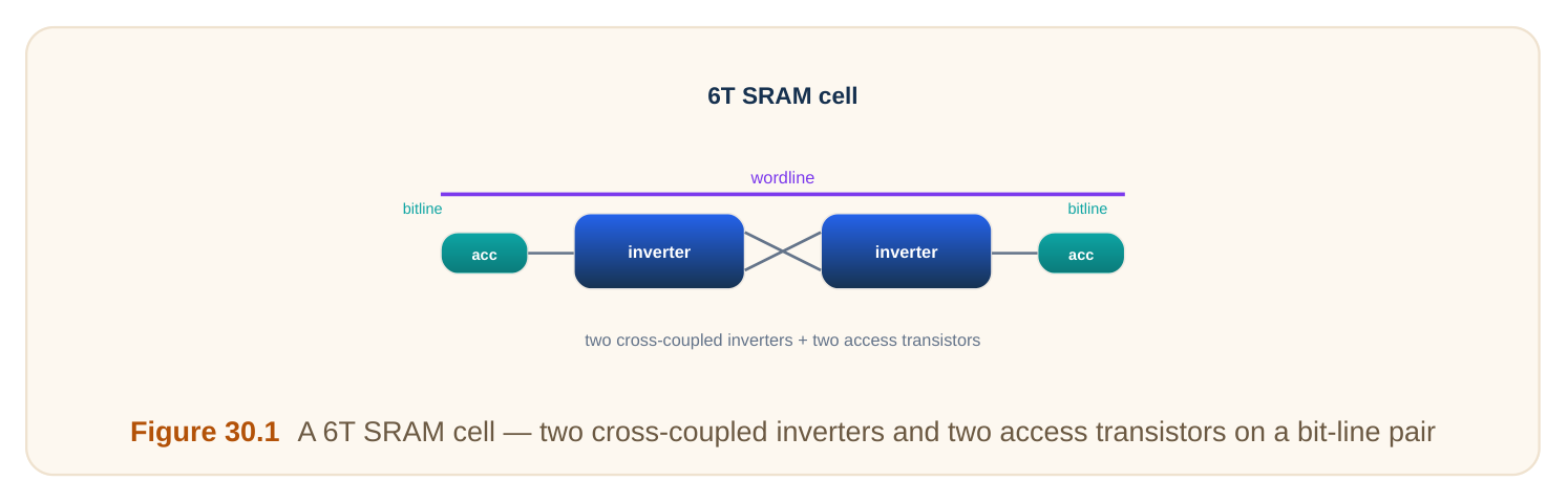
The 6T Cell
A single SRAM bit uses six transistors. Two cross-coupled inverters form a loop that holds the bit: each feeds the other, so the pair locks into one of two stable states. Two more transistors, the access transistors, connect the cell to a pair of bit-lines when the word-line turns on. The cell holds its value as long as power is on. That is why it is "static" — no refresh needed, unlike DRAM. The price is six transistors per bit, so SRAM is fast but area-hungry.
| Part | Count | Job |
|---|---|---|
| Cross-coupled inverters | 4 transistors | hold the bit |
| Access transistors | 2 transistors | connect to bit-lines |
Reading Without Destroying
To read, both bit-lines are first precharged high. Then the word-line turns on the access transistors. The side of the cell holding a low gently pulls its bit-line down a little. So a tiny voltage difference appears between the two bit-lines — one stays high, the other droops. The danger is that the read action can disturb the stored value. The bit-line, sitting high, pushes back on the low node inside the cell through the access transistor. If it pushes too hard, the cell can flip. The defence is sizing: the internal pull-down transistor is made stronger than the access transistor, so the cell holds firm. This ratio is the read stability margin.
Worked example — read differential
A bit-line is precharged to 1.0 V. During a read, the cell discharges it at about 0.4 V per nanosecond, and the sense amplifier needs an 80 mV gap.
time to develop 80 mV = 0.080 V / 0.4 V/ns = 0.20 nsJust 0.2 ns to make a readable gap. The sense amplifier then fires. Waiting longer than needed wastes time; firing too early misreads. Timing the sense amplifier is critical.
Sense Amplifiers
A full bit-line swing — pulling the line all the way from high to low — would be slow and burn power, because bit-lines are long and heavy. Instead, the cell only nudges the bit-line a little. A sense amplifier then detects that small difference and snaps it to a full logic level fast. A common type is a cross-coupled latch that, once enabled, amplifies whichever input is slightly higher into a full high and pulls the other to full low. It turns an 80 mV whisper into a clean 1 and 0 in a fraction of a nanosecond. This is the secret to fast, low-power reads.
| Approach | Speed | Power |
|---|---|---|
| Full bit-line swing | slow | high |
| Small swing + sense amp | fast | low |
Worked example — power saved by small swing
A bit-line has 200 fF. Full swing is 1.0 V; small-swing read moves only 0.1 V.
full swing energy ∝ C × V = 200f × 1.0 = 200 fC moved
small swing       ∝ 200f × 0.1 = 20 fC moved
~10× less charge per read on the bit-line
Across millions of reads, that 10× saving on bit-line activity is huge.
Writing a Cell
To write, the bit-lines are driven to the new value: one forced high, the other low. The word-line turns on. Now the bit-lines must overpower the cell's holding loop and flip it to the new state. This is the opposite need from reading. For a safe read you want the cell to resist the bit-lines. For a safe write you want the bit-lines to win. These two goals pull the sizing in opposite directions, which is the core tension of SRAM design. The write margin is how reliably the bit-lines can flip the cell.
| Operation | What must win | Margin name |
|---|---|---|
| Read | the cell (hold) | read stability |
| Write | the bit-lines (flip) | write margin |
Write Assist
As cells shrink and voltage drops, writes get hard: the bit-lines struggle to flip a stubborn cell. Writeassist tricks help the bit-lines win without hurting read stability. Common assists: lower the cell's supply briefly during a write (a weaker cell is easier to flip); boost the word-line a little (stronger access transistors); or drive the low bit-line below ground for a moment (a harder pull). Each gives the write side an edge only when writing, leaving reads untouched.
| Write assist | Effect |
|---|---|
| Lower cell supply | weakens hold loop, easier flip |
| Boost word-line | stronger access transistors |
| Negative bit-line | harder pull on the cell |
Worked example — voltage and write margin
At 0.9 V a cell writes with comfortable margin. At 0.6 V the margin nearly vanishes. Dropping the cell supply by 0.1 V during the write:
effective hold strength ∝ supply
0.6 → 0.5 V during write ≈ 17% weaker hold loop
→ bit-lines now flip the cell reliably
A brief, small supply dip restores the write margin at low voltage.
The Support Logic Around the Array
A memory is not just cells. Around the array sit the circuits that make it usable.
- Address decoder: turns an address into a single active word-line, selecting one row.
- Bit-line precharge: charges the bit-lines high before each access.
- Column multiplexer: picks which columns connect to the sense amplifiers and write drivers, so one set serves many columns.
- Write drivers and sense amplifiers: do the actual writing and reading. Leakage matters too. In a large array, the vast majority of cells are idle at any moment, but they all leak. So low-leakage cell design and techniques like lowering idle supply are vital for big memories.
Worked example — decoder size
A memory has 1024 rows. How many address bits select a row?
rows = 2^n → 1024 = 2^10 → n = 10 address bits
the row decoder turns 10 bits into 1 of 1024 word-lines
Interview Q&A
transistors) form a loop that locks into one of two stable states and holds the bit, plus two access transistors connect it to the bit-lines via the word-line. It is static because it keeps its value as long as power is on, needing no refresh — unlike DRAM.
high, the word-line turns on, and the low side of the cell droops its bit-line slightly, creating a small differential. The risk is that the high bit-line pushes back on the cell's low node through the access transistor and flips it; sizing the internal pull-down stronger than the access transistor preserves read stability.
swinging them fully is slow and power-hungry. A sense amplifier detects a small (e.g. 80 mV) difference and snaps it to full logic levels quickly, giving fast reads and roughly an order of magnitude less bit-line charge per read.
must resist the bit-lines so it is not disturbed, which wants a strong cell. For a safe write the bit-lines must overpower and flip the cell, which wants a weak cell. Balancing these opposing read-stability and write-margin needs is the core tension of SRAM design.
writes without hurting reads. Methods include briefly lowering the cell supply (weakening the hold loop), boosting the word-line (stronger access transistors), or driving the low bit-line slightly below ground for a harder pull.
the address; bit-line precharge sets the lines high before access; a column multiplexer shares sense amps and write drivers across many columns; and write drivers and sense amplifiers perform the actual writes and reads. Low-leakage design also matters because idle cells dominate a large array.
Key Takeaways
- The 6T cell holds a bit in two cross-coupled inverters; two access transistors connect it to the bit-line pair.
- Reads develop a tiny bit-line differential; the internal pull-down must beat the access transistor for read stability.
- Sense amplifiers turn a small swing into full levels — fast reads with ~10× less bit-line charge.
- Read wants a strong cell, write wants a weak cell — opposing needs are SRAM's central trade- off.
- Write assist (lower cell supply, boosted word-line, negative bit-line) restores write margin at low voltage; decoders, precharge, and column muxes surround the array.
Comments
Leave a Reply