 ChipBuddy
← Home
ChipBuddy
← Home
Fabrication & Layout Basics
From Drawing to Silicon
A chip starts as drawings. It ends as patterned silicon. In between, a factory builds the chip layer by layer. A designer does not need every physics detail. But a clear mental model helps a lot. It explains why design rules exist. It explains why layout looks the way it does. This chapter gives that model in plain terms.
How Chips Are Made (the Short Version)
Think of building a chip like printing many stencil layers on a wafer. A wafer is a thin disc of silicon. The factory repeats a few steps for each layer.
- 1. Add a thin film (grow or deposit a material).
- 2. Coat it with a light-sensitive layer (photoresist).
- 3. Shine light through a mask (a stencil that holds the pattern).
- 4. Wash away the exposed (or unexposed) resist.
- 5. Etch or implant where the resist is gone.
- 6. Strip the leftover resist. Repeat for the next layer.
This light-printing step is photolithography (patterning a layer using light and a mask). Each mask defines one layer's shapes. A modern chip needs dozens of masks. Masks are very expensive. That is why a small fix that needs new base masks costs a lot.
| Step | Plain meaning |
|---|---|
| Deposit/grow | add a thin material film |
| Photoresist | light-sensitive coating |
| Expose (litho) | print the mask pattern with light |
| Etch/implant | carve or dope the pattern |
| Strip | remove leftover resist |
The Layers a Designer Sees
A CMOS layout is made of a fixed set of layers. Each has a job.
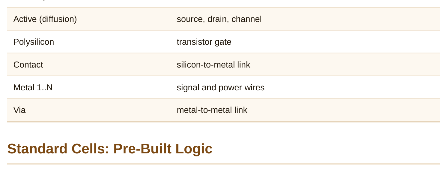
- Wells (n-well / p-well): large tubs of doped silicon. PMOS sits in an n-well. NMOS sits in a p-well.
- Active / diffusion: where transistors and their source/drain regions form.
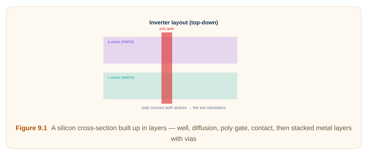
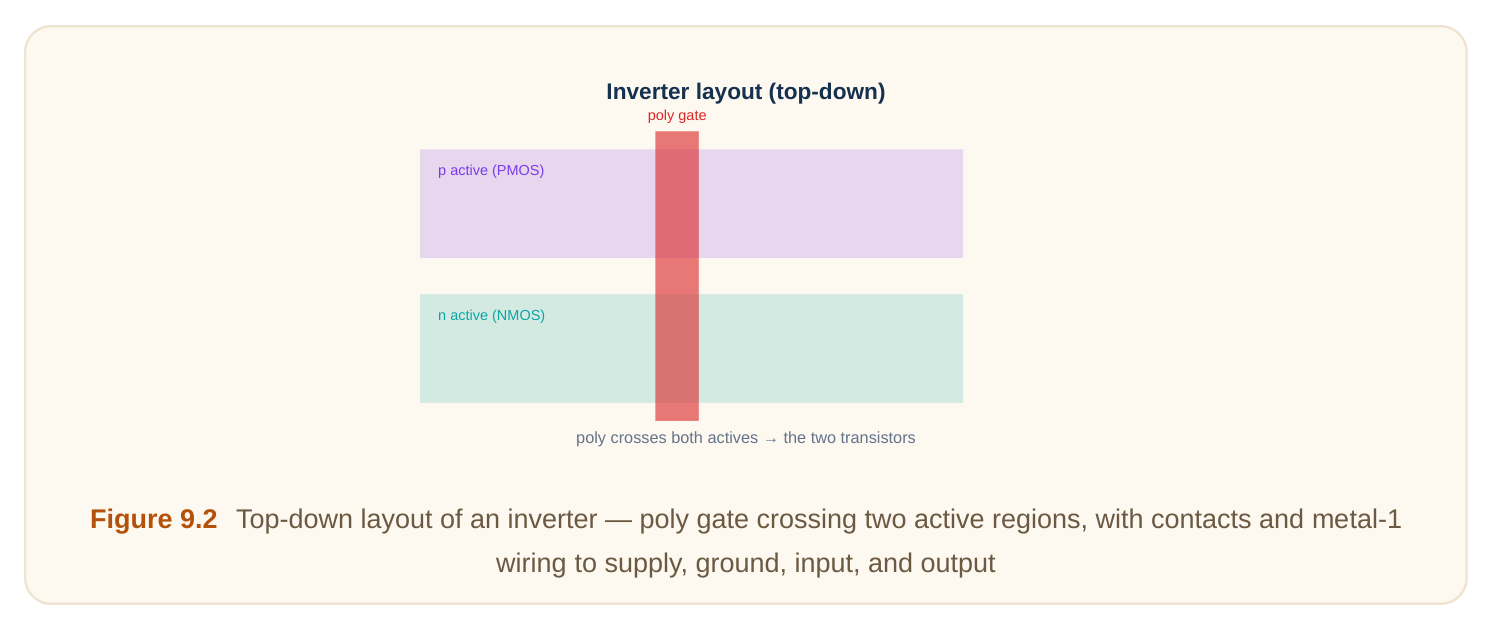
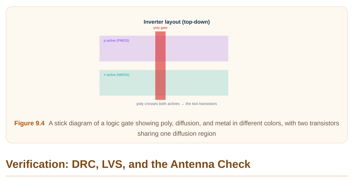
- Polysilicon (poly): the gate material. Where poly crosses active, a transistor forms.
- Contacts: tiny vertical links from silicon up to the first metal.
- Metal layers (M1, M2, …): the wires that connect everything.
- Vias: vertical links between two metal layers. The key picture: poly crossing active makes a gate. Contacts and vias stitch the layers together. Metal carries the signals.
| Layer | Role |
|---|---|
| n-well / p-well | tubs that hold PMOS / NMOS |
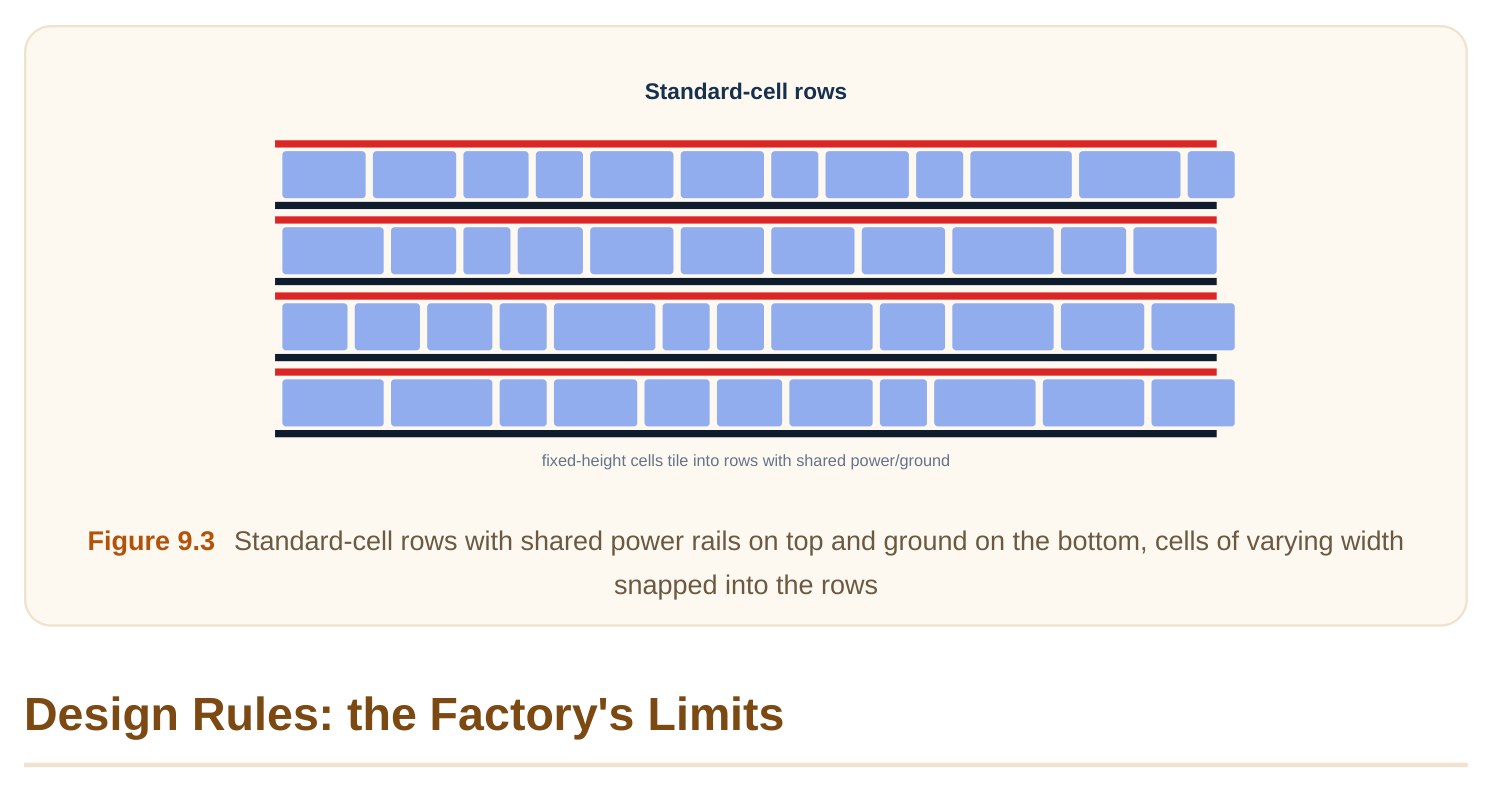
Designers rarely draw each transistor. Instead they use standard cells. A standard cell is a predesigned layout of one gate. Examples: an inverter, a NAND, a flip-flop. All cells in a library share the same height. They snap into rows, like books on a shelf. Power runs along the top of each row. Ground runs along the bottom. A placement tool drops cells into these rows. This row system makes automatic layout possible. Cell width varies with the gate. A big driver is wider. A simple inverter is narrow. But the height stays fixed. That shared height is what lets cells tile cleanly.
The factory cannot print perfect shapes. Lines blur. Layers can misalign. So the foundry (the chip factory) gives design rules. These are minimum sizes and spacings you must obey. Common rule types:
- Minimum width: a shape cannot be thinner than this, or it may break.
- Minimum spacing: two shapes must stay this far apart, or they may merge.
- Minimum enclosure: one layer must overlap another by this much (e.g., metal around a via).
- Minimum area: a shape must not be too tiny. Break a rule and the chip may not build correctly. So a tool checks every shape against the rules. That check is DRC (design-rule check). It flags any violation. Rule type What it limits Why Width thinnest line avoid breaks Spacing gap between shapes avoid shorts/merges Enclosure overlap of layers reliable contacts/vias Area smallest shape printability
Worked example — a spacing check
Say the metal-1 spacing rule is 0.05 µm (micrometers). Two wires are drawn 0.04 µm apart. That is below the rule. DRC flags it. You must move them at least 0.01 µm farther apart. Now the gap is 0.05 µm. The check passes.
Stick Diagrams and Shared Diffusion
Before exact layout, designers sketch a stick diagram. It is a quick, color-coded cartoon of a layout. Poly is one color. Diffusion is another. Metal is another. It shows the plan without exact sizes. A key trick is shared diffusion (two transistors sharing one source/drain region). If two transistors abut, they can share a diffusion edge. That removes a contact and saves width. Good cell layouts share diffusion wherever the logic allows.
Worked example — area from sharing
Suppose four transistors sit in a row. Each unshared transistor needs its own diffusion strip, say 5 units wide each, totaling 20 units. If neighbours share diffusion, adjacent strips merge. The row might shrink to about 14 units. That is a 30% area saving, just from sharing. This is why diffusion sharing is a core layout skill.
Three checks protect a layout.
- DRC (design-rule check): are all shapes legal for the factory? (covered above)
- LVS (layout-versus-schematic): does the drawn layout match the intended circuit? It compares the layout's devices and connections to the schematic. A mismatch means a wiring error.
- Antenna check: during fabrication, long metal connected only to a gate can collect charge. That charge can damage the thin gate. The fix is to add a small diode or break the metal. The antenna check finds risky nets. Pass all three and the layout is ready. Skip them and you risk a dead chip.
| Check | Question it answers |
|---|---|
| DRC | are shapes factory-legal? |
| LVS | does layout match the circuit? |
| Antenna | will charge harm a gate during build? |
Interview Q&A
deposits a film, prints a pattern with light and a mask (photolithography), then etches or dopes the pattern. Dozens of masks stack up to form transistors and wires.
crosses an active/diffusion region. The poly is the gate. The diffusion on each side becomes source and drain. PMOS sits in an n-well; NMOS sits in a p-well.
share one height so they tile into rows with shared power and ground rails. That fixed height is what lets placement tools drop cells in rows and build large designs automatically.
width, spacing, and enclosure rules, so the chip can be built. LVS checks that the drawn layout matches the intended schematic, so the wiring and devices are correct. You need both before tapeout.
only to a gate can collect charge. That charge can damage the thin gate oxide. Fixes include adding a small protection diode or routing part of the net on a higher layer to break the antenna. An antenna check flags the risky nets.
Key Takeaways
- Chips are built layer by layer using photolithography (printing patterns with light and masks); masks are costly, so base-layer changes are expensive.
- The designer's layers are wells, active/diffusion, poly, contacts, metal, and vias; a transistor forms where poly crosses active.
- Standard cells are pre-built gate layouts of fixed height that tile into rows with shared power/ ground rails.
- Design rules (width, spacing, enclosure, area) reflect factory limits; DRC checks them.
- Verify with DRC, LVS, and the antenna check; shared diffusion and stick diagrams are key area- saving layout skills.
Comments
Leave a Reply