 ChipBuddy
← Home
ChipBuddy
← Home
Interconnect — Wires, R, C & Delay
Delay
Why Wires Now Matter as Much as Gates
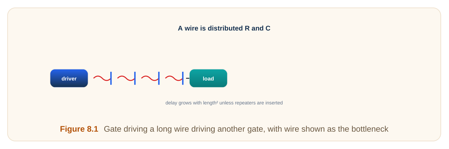
A chip is more than transistors. It is also wires. Wires (thin metal lines that connect gates) carry every signal. Years ago, wires were almost free. Gates were slow, and wires kept up easily. That has changed. Transistors got tiny and fast. Wires got tiny too, but not faster. A thin wire is a slow wire. So today, wire delay (the time a signal needs to travel a wire) can rule the clock. On a long path, the wire may be slower than the gates it links. Think of a relay race. The runners (gates) are fast. But the track (the wire) got long and muddy. Now the track sets the pace. This chapter explains why. We cover wire resistance, wire capacitance, their product (RC), crosstalk, the metal stack, and electromigration.
Wire Resistance
Resistance (opposition to current flow) lives in every wire. A wire's resistance depends on its shape. The formula is simple: R = (rho × L) / (W × T) Here rho is resistivity (a material constant, lower is better), L is length, W is width, and T is thickness. Read it plainly. Longer wires have more resistance. Wider or thicker wires have less. Cross-section (width times thickness) is the path for current. Picture a water pipe. A long pipe resists flow. A fat pipe lets water rush through. Engineers often use sheet resistance (resistance per square, written R_sheet). Then: R = R_sheet × (L / W) The ratio L/W is the number of squares. Each square adds the same resistance, no matter its size.
| Factor | Effect on Resistance | Plain reason |
|---|---|---|
| Longer length (L) | Higher R | More metal to push through |
| Wider width (W) | Lower R | Bigger path for current |
| Thicker metal (T) | Lower R | Bigger path for current |
| Higher resistivity (rho) | Higher R | Metal fights the current more |
| Smaller node | Higher R | Wires shrink, paths narrow |
Copper replaced aluminum to lower rho. Copper resists less, so wires stay faster. There is a hidden problem at tiny nodes. Wires get so narrow that electrons bump the sidewalls. This is called surface scattering. It raises the effective resistivity above the bulk value. So a wire at a small node resists more than its size alone suggests. Thin barrier liners around the copper make it worse. The pure copper core shrinks. This is one reason wire delay refuses to scale down. Each generation, wires fight harder against the current.
Wire Capacitance
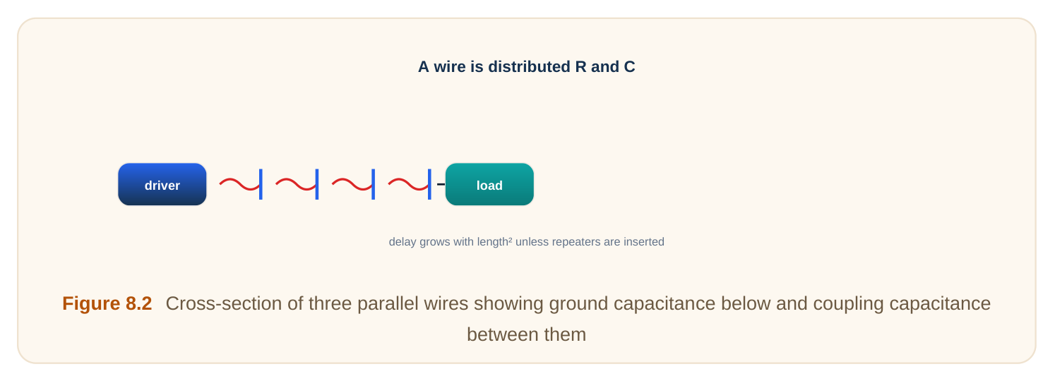
A wire also stores charge. That makes it a capacitor (a charge holder). Capacitance (ability to store charge) comes in two flavors. First, capacitance to ground. The wire sits above the silicon. Charge builds between them. Second, capacitance to neighbors. Nearby wires sit beside yours. Charge builds across the gap. Both must be charged and drained when a signal flips. That takes time and energy. At modern nodes, wires are tall and packed close. So neighbor capacitance often beats ground capacitance. Sidewalls dominate.
| Capacitance type | Where it forms | When it grows |
|---|---|---|
| To ground (area) | Wire over substrate | Wider wire, thinner gap below |
| To neighbor (coupling) | Wire to side wire | Closer spacing, taller wires |
| Fringe | Edges of the wire | Always present, hard to remove |
Total wire capacitance is the sum. More capacitance means slower switching. There is also a third small piece called fringe capacitance. It forms at the edges and corners of the wire. The field bulges outward there. Fringe capacitance is hard to remove. It stays even when wires are far apart. At small nodes it is a real share of the total. One more idea matters here. The dielectric (the insulator between wires) sets how strong the capacitance is. A low-k dielectric (an insulator with a small dielectric constant) stores less charge. Foundries push for low-k materials. Less charge stored means faster wires. It is a direct way to cut wire capacitance.
The RC of a Wire and Why Delay Grows With Length Squared
Now combine R and C. Together they set delay.
A short wire is easy. Treat R and C as single lumps. Delay is roughly R × C. A long wire is harder. Resistance and capacitance spread along the whole line. This is a distributed RC line (resistance and capacitance smeared evenly). Here is the key fact. For a distributed wire, delay grows with the square of length. Why squared? Both R and C grow with length. R doubles when length doubles. C also doubles. Their product grows fourfold. A common estimate for distributed delay is: t = 0.38 × R × C Here R and C are the total wire values. Since each scales with L, the product scales with L². Double the wire, and delay roughly quadruples. That is brutal for long wires. Why the 0.38 factor? A distributed line is not one lump. The charge fills it gradually, from near end to far end. So it responds faster than a single lumped RC. A lumped model would use a factor near 0.69 for the same swing. The distributed factor of 0.38 reflects the smeared, gradual fill. It is the more honest model for a real wire. The lesson stands either way. The L² term is the enemy. Keep wires short, or break the square law with the trick below.
Worked Example 1: Estimate Wire RC Delay
Let us put numbers to it. A wire is 2 mm long. Resistance per mm is 250 ohms. Capacitance per mm is 200 fF (femtofarads). Total resistance: R = 250 × 2 = 500 ohms. Total capacitance: C = 200 × 2 = 400 fF = 0.4 pF. Distributed delay: t = 0.38 × R × C. t = 0.38 × 500 × 0.4e-12 = 0.38 × 200e-12 = 76 ps (picoseconds). Now double the length to 4 mm. R becomes 1000 ohms. C becomes 800 fF. t = 0.38 × 1000 × 0.8e-12 = 304 ps. Length doubled, but delay rose 4x. That is the square law in action.
Repeaters: Making Square Delay Linear
We cannot accept squared delay on long wires. The fix is repeaters. A repeater (a buffer inserted along a wire) splits the wire into pieces. Each piece is short. Each piece has small delay. Why does this help so much? Each short piece pays only its own small RC. The square law applies per segment, not to the whole.
Add the segment delays. Plus add buffer delays. The total now grows roughly linearly with length, not as the square. Picture a long water line with weak pressure. Add pump stations along the way. Each pump pushes water to the next. Flow stays strong end to end. There is a sweet spot. Too few repeaters, and segments stay long. Too many, and buffer delay piles up. Tools find the best number and size.
| Technique | What it does | Effect on delay |
|---|---|---|
| Insert repeaters | Splits wire into short pieces | Square delay becomes near-linear |
| Widen the wire | Lowers resistance | Cuts RC, helps long wires |
| Use upper metal layer | Thicker, lower R and C | Faster long wires |
| Increase spacing | Cuts coupling capacitance | Less delay and less crosstalk |
| Shorten the route | Less L means less R and C | Big win, fewer squares |
Worked Example 2: Repeaters Cut Long-Wire Delay
Take a long wire. Without repeaters, its distributed delay is 800 ps. Now split it into 4 equal segments with 3 repeaters. Each segment is 1/4 the length. So each segment's R and C are 1/4 of the whole. Each segment's RC delay is (1/4 × 1/4) = 1/16 of the original. One segment delay: 800 / 16 = 50 ps. Four segments: 4 × 50 = 200 ps. Now add buffer cost. Each repeater adds 30 ps. Three repeaters add 90 ps. Total with repeaters: 200 + 90 = 290 ps. That beats 800 ps by a wide margin. Repeaters turned a square cost into a near-linear one. There is a cost to pay. Repeaters use area and burn power. Each buffer leaks and switches. A chip can hold millions of them. So designers balance speed against power. They place just enough repeaters to meet timing. More than that wastes energy. Tools size and space them automatically.
Coupling Capacitance and Crosstalk
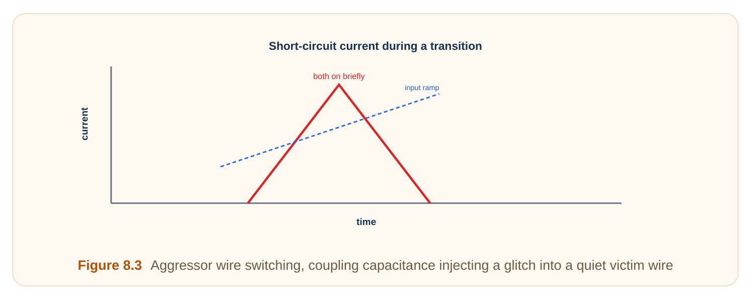
Wires sit close. So they talk to each other. This is crosstalk (unwanted coupling between wires). Here is the cause. Your wire shares coupling capacitance with a neighbor. When the neighbor switches, it tugs charge onto your wire. Two bad things can happen. First, a glitch. A quiet wire gets a false bump. If big enough, it looks like a real signal.
Second, a delay change. If the neighbor switches the opposite way, your wire slows down. If it switches the same way, your wire speeds up. Think of two ropes lying side by side. Shake one rope. The other rope shivers too. That shiver is crosstalk. The worst case is the Miller effect. When two wires switch in opposite directions, the effective coupling capacitance doubles. Delay can spike hard.
| Crosstalk effect | Cause | Result |
|---|---|---|
| Glitch (noise) | Neighbor switches, victim quiet | False pulse, possible wrong value |
| Slowdown | Neighbor switches opposite way | Victim signal arrives late |
| Speedup | Neighbor switches same way | Victim signal arrives early |
How do we fight crosstalk? Add spacing. Add shield wires (grounded lines between signals). Avoid long parallel runs. Stagger switching times.
The Metal Layer Stack
A chip has many metal layers stacked above the transistors. This is the metal stack. The layers are not the same. They follow a clear pattern. Lower layers are thin and packed tight. They sit close to the transistors. They handle short, local connections. Upper layers are thick and widely spaced. They sit far above. They handle long, global connections. Why this design? Thin lower layers pack dense routing. Many short wires fit. But they are resistive and slow. Thick upper layers have low resistance. They carry signals fast over long distances. So long and global wires go up high.
Vias (vertical metal plugs) connect one layer to the next. A signal climbs up for a long trip, then drops back down.
| Layer group | Thickness | Pitch (spacing) | Best for |
|---|---|---|---|
| Lower (local) | Thin | Tight | Short cell-to-cell wires |
| Middle (intermediate) | Medium | Medium | Block-level routing |
| Upper (global) | Thick | Wide | Long wires, clock, power |
The rule of thumb is simple. Short signal, low layer. Long signal, high layer. Metal stack: thin low, thick high M6 (thick) M5 M4 M3 M2 M1 (thin) long global wires go on thick upper layers
Figure 8.4 Side view of metal stack, thin layers near transistors, thick layers on top, vias connecting them
Worked Example 3: Thin Layer vs Thick Layer
Compare the same 1 mm wire on two layers. On a thin lower layer: R per mm is 400 ohms, C per mm is 200 fF. R = 400 ohms. C = 200 fF. Delay = 0.38 × 400 × 200e-15 = 30.4 ps. On a thick upper layer: R per mm is 80 ohms, C per mm is 180 fF. R = 80 ohms. C = 180 fF. Delay = 0.38 × 80 × 180e-15 = 5.5 ps. The thick layer is over 5x faster. The reason is mostly lower resistance. This is why designers push long wires up high. The thick metal pays off.
Electromigration and Wide Power Wires
Wires can wear out. The cause is electromigration. Electromigration (slow erosion of metal by current) happens at high current. Moving electrons bump metal atoms. Over time, atoms drift away. The result is damage. Thin spots form. Voids open. Eventually the wire breaks. Or metal piles up and shorts to a neighbor. Picture a river eroding its bank. Water carries soil away grain by grain. Years later, the bank gives way.
Electromigration depends on current density (current per unit area). Pack too much current into a thin wire, and erosion speeds up. Which wires carry the most current? Power wires and clock wires. Power lines feed the whole chip. Clock lines drive huge loads at high speed. So these wires are made wide. A wide wire spreads current over more metal. Current density drops. The wire lasts.
| Wire type | Current level | Width choice | Reason |
|---|---|---|---|
| Signal wire | Low, brief | Narrow | Little current, low erosion risk |
| Clock wire | High, constant | Wide | Heavy switching, must survive |
| Power/ground | Very high, steady | Very wide | Feeds whole chip, must not fail |
Designers also follow current limits from the foundry. Each layer has a safe current per width. Stay under it, and the chip lives for years.
Interview Q&A
Both resistance and capacitance grow with length. Resistance doubles when length doubles. Capacitance also doubles. Delay depends on their product, R times C. So the product grows fourfold when length doubles. That is the square law for a distributed RC wire.
Repeaters split the wire into short segments. Each segment has small R and C, so small delay. The square law now applies per segment, not to the whole wire. Total delay becomes roughly linear with length. Buffers add some fixed cost, but the net delay drops sharply on long wires.
Crosstalk is unwanted coupling between wires through their shared capacitance. A switching neighbor tugs charge onto a quiet wire. This can cause a false glitch or change the wire's delay. To reduce it, add spacing, insert grounded shield wires, avoid long parallel runs, and stagger switching times.
Upper layers are thick and widely spaced. Thick metal has low resistance. Wide spacing lowers coupling capacitance. Both cut RC delay. So long wires run fast on upper layers. Lower layers are thin and dense, good only for short local connections, since they are resistive and slow.
They carry high current. High current density drives electromigration, which slowly erodes metal and can break a wire. A wide wire spreads current over more metal, lowering current density. This keeps erosion slow and the wire reliable over the chip's life. Wide clock wires also lower resistance, helping timing.
Key Takeaways
- Wires now matter as much as gates. At small nodes, wire delay can dominate the path.
- Wire resistance grows with length and shrinks with cross-section. Width and thickness lower it.
- Wire capacitance forms to ground and to neighbors. At small nodes, neighbor coupling often dominates.
- A long wire is a distributed RC line. Its delay grows with the square of length.
- Repeaters split the wire into short segments. They turn square delay into near-linear delay.
- Crosstalk is coupling between wires. It causes glitches and delay changes. Spacing and shielding help.
- The metal stack has thin dense lower layers and thick fast upper layers. Long wires go up high.
- Electromigration slowly erodes metal at high current. Power and clock wires are made wide to survive it.
Comments
Leave a Reply