 ChipBuddy
← Home
ChipBuddy
← Home
Combinational Circuit Families
Why More Than One Style?
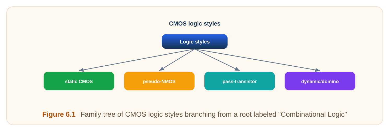
Static CMOS is the default way to build logic. It is robust and easy. But it is not always the smallest or the fastest. Engineers have other circuit styles too. Each style trades one good thing for another. This chapter tours those styles. We start with plain static CMOS. Then we look at ratioed logic, passtransistor logic, transmission gates, dynamic logic, and domino logic. We close with trade-offs and when to pick each. A combinational circuit (logic whose output depends only on current inputs, with no memory) can be built many ways. The truth table stays the same. Only the transistors change.
Static CMOS: The Reliable Default
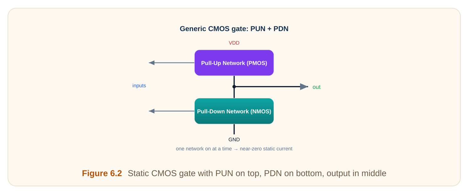
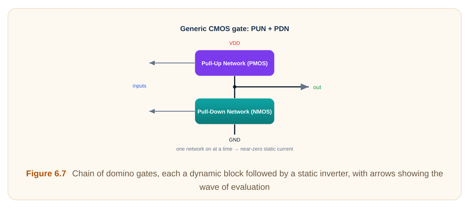
Static CMOS uses two networks. A pull-up network (PUN) of PMOS transistors connects the output to VDD (supply voltage). A pull-down network (PDN) of NMOS transistors connects the output to ground. The two networks are complementary. Only one conducts at a time. This gives a full swing. The output reaches a clean 0 or a clean VDD. There is no DC (steady-state) current path from supply to ground. So static power is tiny. But there is a cost. Each input drives both a PMOS and an NMOS. So a gate with N inputs needs 2N transistors. That is a lot of area. Also, static CMOS gates are naturally inverting. They produce NAND, NOR, and AOI (and-or-invert) shapes. A plain AND or OR needs an extra inverter. Think of static CMOS as a sturdy two-way valve. One side always seals while the other opens. Nothing leaks, but you need two valves per knob.
Ratioed Logic: Pseudo-NMOS
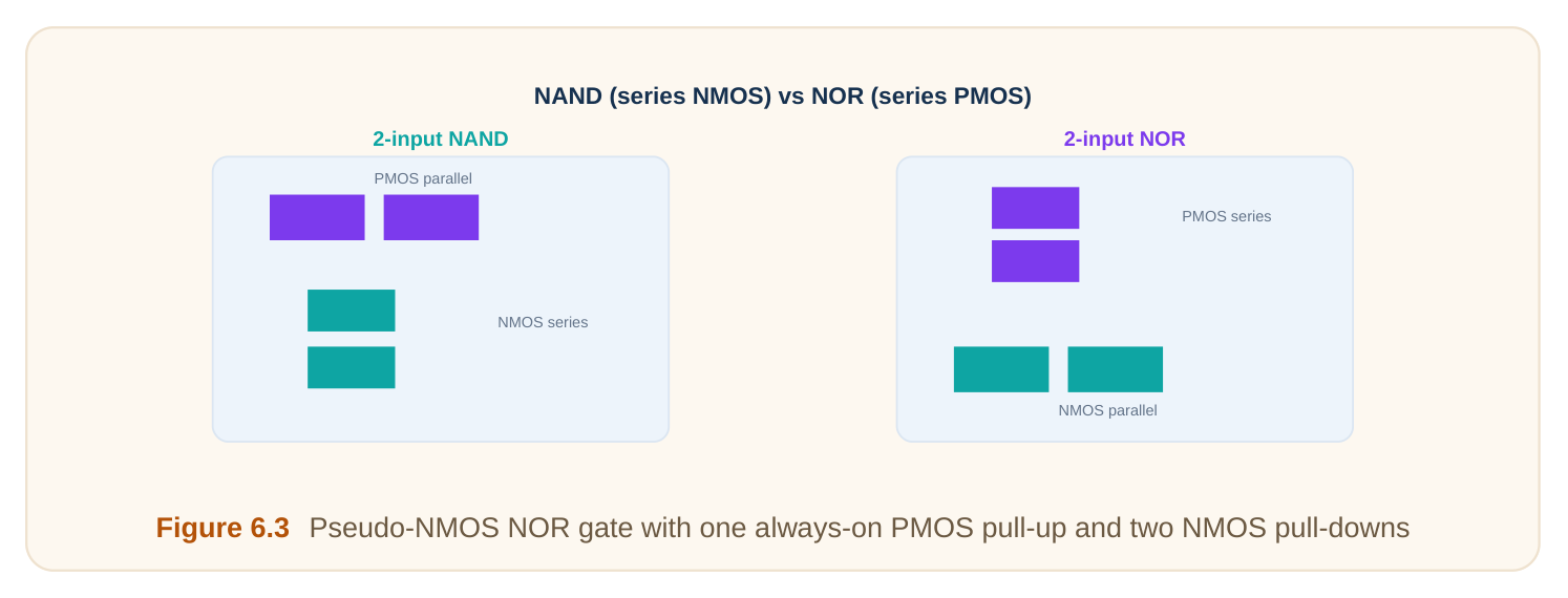
Pseudo-NMOS drops the full PMOS network. It keeps the NMOS pull-down network. For the pull-up, it uses a single PMOS with its gate tied to ground. This PMOS is always on. It acts like a weak resistor to VDD. The transistor count falls a lot. A NOR gate needs only N+1 transistors instead of 2N. The gate stays non-inverting issues aside, it is still inverting in shape, but it is compact. Here is the catch. When the output is low, both the always-on PMOS and the NMOS path conduct. So a DC current flows from VDD to ground. This burns static power all the time the output is low. There is also a ratio problem. The output low voltage is set by the strength ratio of the NMOS to the PMOS. We must size the NMOS much stronger than the PMOS. If the ratio is wrong, the "low" is not low enough. This weakens the noise margin (the safety gap between a valid logic level and the switching point). The name "ratioed" comes from this need to tune sizes. Static CMOS is "ratioless" because its low and high are guaranteed by the structure, not by sizing.
Pass-Transistor Logic
Pass-transistor logic uses transistors as switches. The input signal passes through the transistor channel to the output. The gate terminal acts as the control. This can save many transistors. A 2:1 multiplexer (a switch that picks one of two inputs) can use just two NMOS pass transistors. Some XOR designs shrink too. But a single NMOS has a flaw. It passes a strong 0 but a weak 1. An NMOS can only pull the output up to VDD minus a threshold voltage (the minimum gate voltage to turn a transistor on). So a "1" arrives degraded. A single PMOS is the mirror. It passes a strong 1 but a weak 0. Either device alone loses one level. A weak high causes problems. It may not fully turn off the next PMOS stage. That leaks static current. It also shrinks noise margins.
Transmission Gates Fix the Weak Level
A transmission gate is the cure. It places an NMOS and a PMOS in parallel. They share the same channel path but get opposite control signals. When on, both conduct together. Now the NMOS handles the strong 0, and the PMOS handles the strong 1. Together they pass a full swing. No degraded level. The output reaches a clean 0 and a clean VDD. The cost is two transistors per switch instead of one, plus a complemented control signal. But the signal quality is restored. Transmission gates shine in multiplexers, XOR gates, and latches.
Transmission gate (NMOS ∥PMOS) NMOS
in out passes both strong 0 and strong 1 (complementary gates)
Figure 6.4 Transmission gate showing NMOS and PMOS in parallel with complementary gate signals
Comparing the Static Families
The table below sums up the static styles. "Static" here means no clock is needed.
| Style | Pros | Cons | Best use |
|---|---|---|---|
| Static CMOS | Full swing, no static | Large area (2N), inverting current, robust | General logic, default choice |
| Pseudo-NMOS | Fewer transistors, compact | Static current, weak noise margin, ratioed | Wide NOR, ROM lines, PLAs |
| Pass-transistor | Very few transistors | Weak high, threshold drop (NMOS) | Internal nodes, simple muxes |
| Transmission gate | Full swing, compact | Needs complement signal, two muxes | Muxes, XOR, latches devices |
Worked Example 1: A 2:1 Mux From Transmission Gates
We want to build a 2:1 mux. It picks input A when select S is 0. It picks input B when S is 1. Use two transmission gates. The first passes A. The second passes B. For the first gate, the NMOS gate is the inverted select, S-bar. The PMOS gate is S. So when S is 0, S-bar is 1, both turn on, and A passes through. For the second gate, the NMOS gate is S. The PMOS gate is S-bar. So when S is 1, both turn on, and B passes through. Let us count transistors. Each transmission gate is 2 transistors. Two gates make 4. We also need one inverter to make S-bar. That inverter is 2 transistors. Total: 6 transistors. A static CMOS 2:1 mux built from gates needs far more. It uses two AND gates, one OR gate, and an inverter. Roughly 14 to 20 transistors depending on the form. The transmission-gate version wins on area.
Transmission gate (NMOS ∥PMOS) NMOS
in out passes both strong 0 and strong 1 (complementary gates)
Figure 6.5 2:1 mux with two transmission gates and one select inverter
Dynamic Logic: Precharge and Evaluate
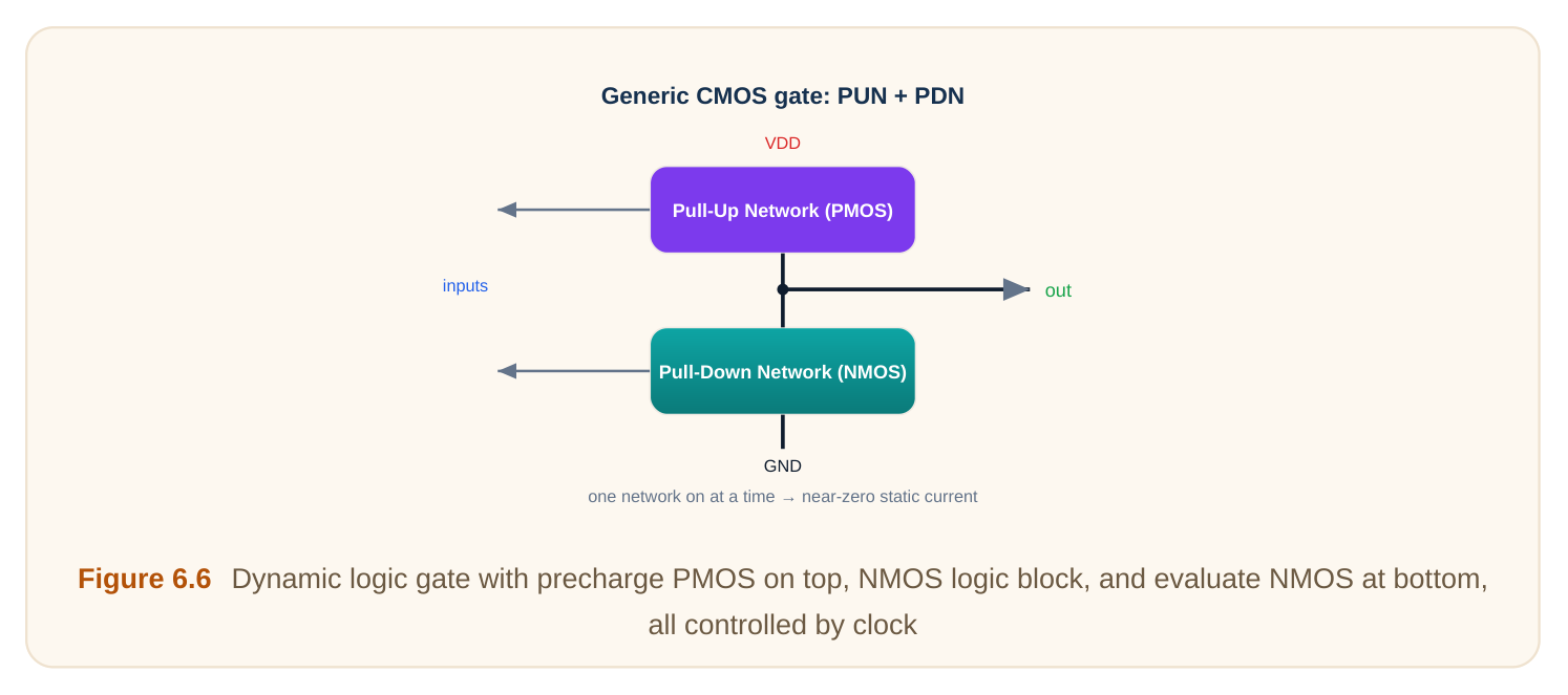
Dynamic logic uses a clock and two phases. It stores the output value as charge on a node. This is like writing on a chalkboard that slowly fades. In the precharge phase, the clock is low. A PMOS pulls the output node up to VDD. The output is now charged high. In the evaluate phase, the clock is high. The precharge PMOS turns off. A clock-controlled NMOS at the bottom turns on. Now the NMOS pull-down network decides. If a path conducts, the output discharges to 0. If no path conducts, the output stays high. Only an NMOS pull-down network is needed. There is no PMOS logic network. So a gate uses N+2 transistors. That is much smaller than 2N. The inputs only drive NMOS gates. So input capacitance is lower and speed is high. But dynamic logic is fragile. Three big problems appear. First is leakage. During evaluate, a high output is held only by stored charge. Leakage current slowly drains it. The high level droops over time. Second is charge sharing. The output charge can spread to internal nodes of the pull-down network. This can pull the output down even when it should stay high. Third is noise. The high node is not actively driven. So input noise can falsely trigger a discharge. There is no PMOS path to fight back.
The Keeper Fixes Some Problems
A keeper is a small weak PMOS. It connects from VDD to the output. Its gate is driven by the output through an inverter. When the output is high, the keeper turns on weakly. It supplies a trickle of current. This replaces charge lost to leakage and charge sharing. It holds the high level. The keeper must be weak. If it is too strong, the pull-down network cannot beat it during a real discharge. So the keeper makes the gate slightly ratioed. It is a small price for much better robustness.
Static vs Dynamic at a Glance
| Feature | Static CMOS | Dynamic logic |
|---|---|---|
| Clock needed | No | Yes |
| Transistors per N-input gate | 2N | N+2 |
| Output drive | Both directions, always | Charge held, not driven high |
| Static power | Very low | Low, plus leakage droop |
| Speed | Moderate | Fast |
| Noise robustness | High | Low, needs keeper |
| Charge sharing risk | None | Yes |
Domino Logic
Plain dynamic gates cannot be chained directly. Here is why. After precharge, every dynamic output is high. During evaluate, an output can only go from high to low. It can fall but never rise.
Now imagine feeding one dynamic output into the next dynamic gate. The next gate's NMOS input sees a high at the start of evaluate. It may discharge wrongly before the first gate settles. This false discharge cannot be undone. The chain breaks. Domino logic solves this. It adds a static inverter after each dynamic gate. The dynamic node precharges high. The inverter output is therefore low at the start of evaluate. A low input cannot wrongly turn on the next NMOS. So the chain is safe. The signals fall in sequence, like a row of dominoes toppling. That is the name. Each stage evaluates, then triggers the next. But there is a strict rule. After the inverter, every domino gate is non-inverting overall. The dynamic part inverts, and the static inverter inverts again. Two inversions cancel. So domino logic can only build non-inverting functions like AND and OR. It cannot directly build NAND or NOR. To get inversion, designers use tricks. They push inversions to the inputs, or use dual-rail domino, which carries both true and complement signals. Dual-rail doubles the gates but restores any function.
Worked Example 2: XOR Transistor Count in Two Styles
XOR (exclusive-OR, true when inputs differ) is a common building block. Let us count transistors in two styles. Style one is static CMOS. A two-input XOR needs the function plus its complements. A full static CMOS XOR built from a complementary gate plus input inverters uses about 12 transistors. The exact number depends on whether complements are already available. Assume they are not: roughly 12 transistors. Style two is transmission-gate XOR. This design uses two transmission gates and one or two inverters. A common form: two transmission gates (4 transistors) plus one inverter to make a complement (2 transistors). Total: about 6 transistors.
So the transmission-gate XOR roughly halves the count. The savings are real. But transmission-gate chains have a weakness. Signals pass through several switches in series. Resistance adds up. Long chains get slow and need buffers.
| Style | Transistors (2-input XOR) | Note |
|---|---|---|
| Static CMOS | ~12 | Robust, full swing, larger |
| Transmission gate | ~6 | Compact, watch series delay |
This shows the core lesson. A smaller count is not free. You pay in delay or robustness somewhere.
The Big Trade-Offs
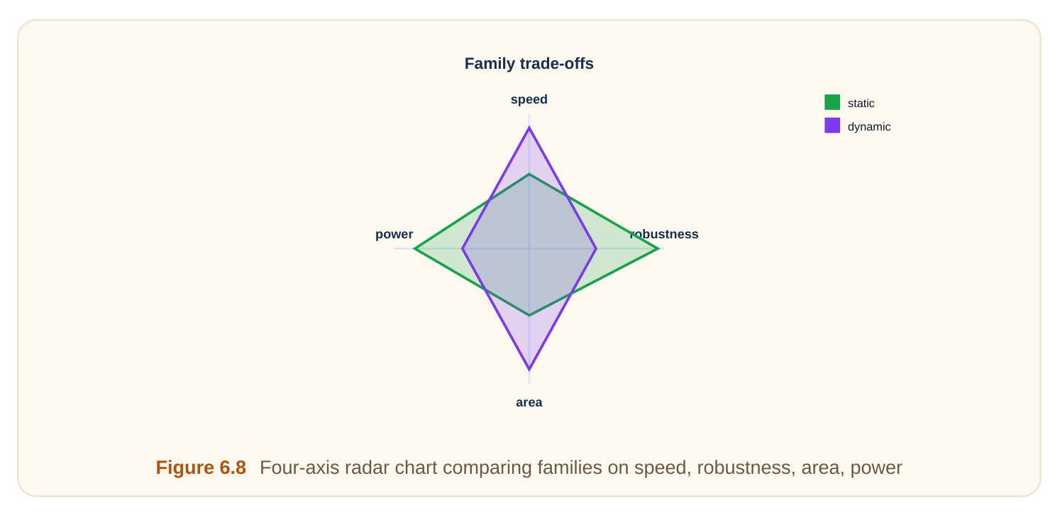
Every family balances four things: speed, robustness, area, and power. Static CMOS wins robustness. It has full swing, strong noise margins, and no clocking worry. It loses on area and is only moderate on speed. Pseudo-NMOS wins area for wide gates. It loses on power because of static current. Pass-transistor and transmission-gate logic win area for muxes and XORs. They risk weak levels and series delay. Dynamic and domino logic win speed and area. They lose robustness. They need careful design, keepers, and clocking.
Why Static CMOS Still Dominates
Despite all the clever alternatives, static CMOS rules most chips. There are clear reasons. First, it is robust by construction. No sizing ratios. No clock timing windows. No charge sharing. It just works.
Second, design tools love it. Standard cell libraries, automatic place-and-route, and timing tools all assume static CMOS. The whole flow is built around it. Third, leakage now dominates power at small nodes. Dynamic logic's leakage droop becomes a serious risk. Static CMOS handles low activity better. Fourth, the speed gap has shrunk. Modern static cells and good sizing are fast enough for most paths. Exotic styles only pay off in rare, very fast blocks. So designers reach for dynamic or domino logic only in special spots. Examples include wide OR structures, fast adders, and memory address decoders. Everywhere else, static CMOS is the safe and productive choice.
Pass-Transistor Issues Summary
| Issue | Cause | Fix |
|---|---|---|
| Weak high (NMOS) | Threshold drop on pull-up | Use transmission gate or PMOS |
| Weak low (PMOS) | Threshold drop on pull-down | Use transmission gate or NMOS |
| Static leakage | Degraded level does not fully shut next stage | Restore full swing with TG or buffer |
| Series delay | Many switches in a chain | Insert buffers, limit chain length |
| Extra control wires | Transmission gate needs complement | Add local inverter |
Interview Q&A
levels are set by which network conducts. The pull-up and pull-down never fight. So sizes do not set the output levels. Pseudo-NMOS has an always-on PMOS fighting the NMOS network. The low output depends on the strength ratio of NMOS to PMOS. Wrong sizing gives a bad low level. That dependence makes it ratioed.
source voltage drops below the threshold. As the output rises, the source voltage rises. When the output nears VDD minus a threshold, the NMOS shuts off. So it cannot pull the output all the way to VDD. The high is degraded. A transmission gate adds a PMOS to carry the strong 1.
the inverter output is low. The output can only rise during evaluate, from low to high. To feed the next gate safely, the signal must start low and only rise. That behavior is non-inverting. So domino can build AND and OR directly, but not NAND or NOR. Dual-rail or input inversion is needed for general functions.
output, driven by the output through an inverter. When the output is high, the keeper trickles current to replace charge lost to leakage and charge sharing. It must be weak so the pull-down network can still
discharge the node during a real evaluate. A strong keeper would block valid discharges or slow them badly.
need high speed and low input capacitance in a critical block. Good fits are wide-fanin OR gates, fast adder carry chains, and memory decoders. The inputs drive only NMOS, so loading is light and speed is high. But you accept clocking, charge-sharing risk, leakage droop, and lower noise margins. For ordinary logic, static CMOS is safer and easier.
Key Takeaways
- Static CMOS is the default: full swing, robust, no static current, but 2N transistors and inverting.
- Pseudo-NMOS cuts transistors but burns static current and needs careful sizing.
- A single NMOS passes a weak 1; a single PMOS passes a weak 0; transmission gates fix both.
- Transmission gates make compact muxes and XORs with full swing, at the cost of a complement signal.
- Dynamic logic is fast and small but suffers leakage, charge sharing, and noise; keepers help.
- Domino logic chains dynamic gates with inverters and must stay non-inverting overall.
- Every family trades speed, area, power, and robustness; static CMOS dominates because tools, robustness, and leakage all favor it.
Comments
Leave a Reply