 ChipBuddy
← Home
ChipBuddy
← Home
The CMOS Inverter — Transfer Curve & Noise Margins
Margins
The inverter is the heartbeat of CMOS design. Master it, and you understand most digital logic. This chapter studies how its output reacts to its input. We also learn how much electrical noise (unwanted voltage disturbance) a gate can survive.
Why the Inverter Matters
The CMOS inverter has two transistors. One is a PMOS (a switch that turns on with a low gate voltage). One is an NMOS (a switch that turns on with a high gate voltage). Their gates tie together as the input. Their drains tie together as the output. When the input is low, the PMOS pulls the output high. When the input is high, the NMOS pulls the output low. The output is always the opposite of the input. That is why we call it an inverter.
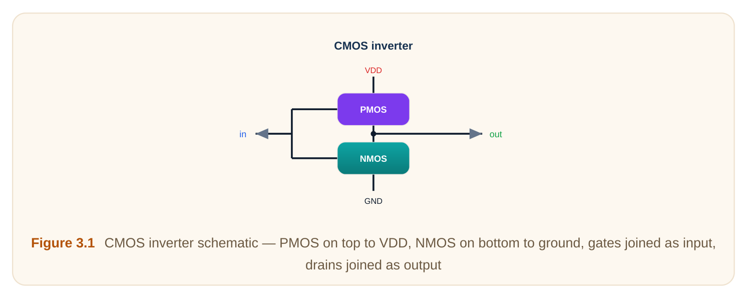
Think of two people holding a rope over a bucket. One pulls the rope up. One pulls it down. Only one pulls hard at a time. The bucket sits high or low depending on who wins. The inverter has another great trait. In a steady state, only one transistor is on. So almost no current flows from supply to ground. The gate uses almost no power when idle. That low static power is why CMOS won over older logic families.
The DC Transfer Curve
The DC transfer curve plots output voltage against input voltage. "DC" means we change the input slowly. We let the output settle each time. The shape of this curve tells us how clean the gate is.
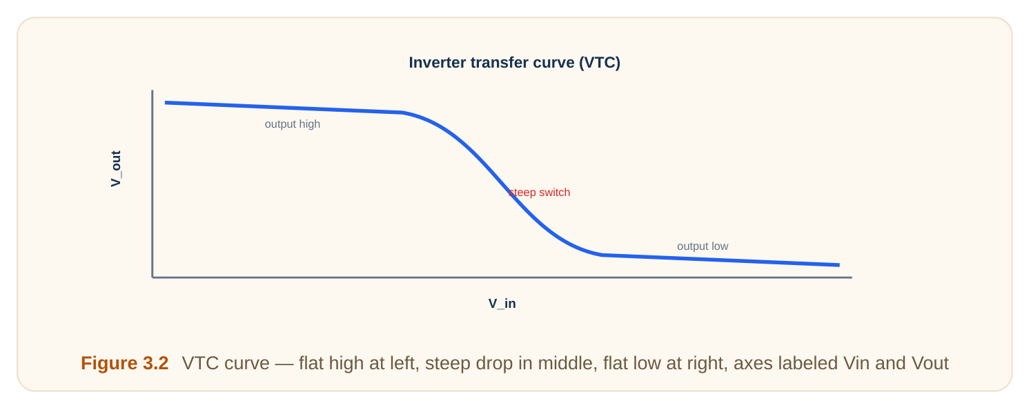
At low input, output stays near the supply voltage (VDD). At high input, output stays near zero. In the middle, the output drops sharply. A sharp middle is good. It means a small input change flips the output fast. We split this curve into five regions. Each region depends on which transistor is on and how it conducts. A MOSFET works in two modes. "Cutoff" means off. "Saturation" means on and acting like a current source. "Linear" (also called triode) means on and acting like a resistor.
TABLE 1: THE FIVE REGIONS OF THE TRANSFER CURVE
| Region | Input range | NMOS state | PMOS state | Output behavior |
|---|---|---|---|---|
| 1 | Vin very low | Cutoff (off) | Linear (resistor) | Output held high at VDD |
| 2 | Vin rising | Saturation | Linear | Output starts to fall slowly |
| 3 | Vin near middle | Saturation | Saturation | Output drops very fast |
| 4 | Vin higher | Linear | Saturation | Output falls toward zero |
| 5 | Vin very high | Linear (resistor) | Cutoff (off) | Output held low at 0 |
Region 3 is the magic zone. Both transistors are in saturation. Both act like strong current sources. A tiny input nudge causes a huge output swing. This gives the curve its steep cliff. Let us walk the regions briefly. At the far left the NMOS is off and the PMOS is wide open. The output is glued to VDD. Raise the input past the NMOS threshold and it starts to pull down, but the PMOS still wins, so the output only dips. Near the middle both pull with equal force and the output collapses fast. Past the middle the NMOS dominates and the output heads to zero. At the far right the PMOS shuts off and the output sticks at zero. Knowing the transistor states in each step is a classic interview test.
The Switching Threshold
The switching threshold (VM) is the special input voltage where output equals input. On the curve, it is where the line crosses the diagonal Vin = Vout. It marks the tipping point of the gate.
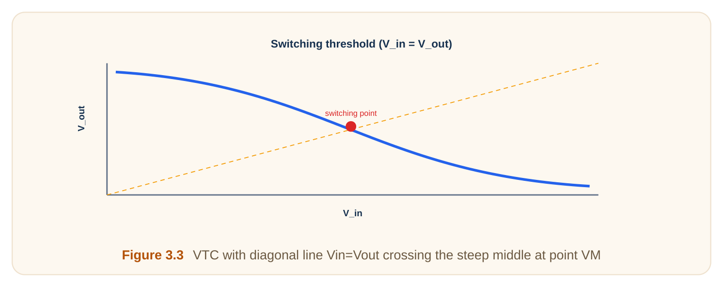
VM matters because it sets where the gate "decides." If VM sits at the middle of the supply, the gate treats highs and lows fairly. That balance gives the best noise protection on both sides. VM depends on transistor strength. Strength comes from the size ratio of the two transistors. We call this the beta ratio. Beta is a measure of how much current a transistor can pass for a given size. A simple rule sums it up. If the PMOS is stronger, it pulls harder toward high. So VM moves up. If the NMOS is stronger, it pulls harder toward low. So VM moves down.
CENTERING VM BY SIZING
Here is a practical problem. Electrons in NMOS move faster than holes in PMOS. So an NMOS of equal size is stronger. To balance them, we make the PMOS wider. The common fix is to widen the PMOS by the mobility ratio. Mobility is how easily charge carriers move. If electrons move about twice as fast as holes, we make the PMOS about twice as wide. Then both transistors pull equally. VM lands near the center.
WORKED EXAMPLE 1: ESTIMATING VM FROM A STRENGTH RATIO
Let us use a supply of VDD = 1.8 V. Let both threshold voltages be 0.4 V in magnitude. Let r be the ratio of PMOS strength to NMOS strength, expressed as the square root of the beta ratio. A handy estimate for VM is: VM = (VTn + r × (VDD − |VTp|)) / (1 + r) Case A: equal strength, so r = 1. VM = (0.4 + 1 × (1.8 − 0.4)) / (1 + 1) VM = (0.4 + 1.4) / 2 VM = 1.8 / 2 = 0.9 V VM equals half the supply. The gate is perfectly centered. Good. Case B: PMOS twice as strong, so r = 2. VM = (0.4 + 2 × 1.4) / (1 + 2) VM = (0.4 + 2.8) / 3 VM = 3.2 / 3 = 1.07 V VM moved up to 1.07 V. A stronger PMOS pulls the tipping point higher. This matches our rule. Case C: NMOS twice as strong, so r = 0.5. VM = (0.4 + 0.5 × 1.4) / (1 + 0.5) VM = (0.4 + 0.7) / 1.5 VM = 1.1 / 1.5 = 0.73 V VM dropped to 0.73 V. A stronger NMOS pulls the tipping point lower. The trend is clear: more PMOS strength raises VM, more NMOS strength lowers it, equal strength centers it.
Logic Levels: VOH, VOL, VIH, VIL
Real circuits do not give perfect highs and lows. We define voltage levels to set limits. Four levels matter most. VOH is the highest output voltage the gate produces for a logic high. VOL is the lowest output voltage for a logic low. These describe what the gate sends out. VIH and VIL describe what the gate accepts as input. VIL is the largest input voltage still read as a low. VIH is the smallest input voltage still read as a high. Between them lies a gray zone the gate dislikes. We find VIH and VIL on the curve at special points. They sit where the curve's slope equals −1. These two points mark the edges of the steep region. Outside them, the output is firmly committed.
TABLE 2: LOGIC-LEVEL DEFINITIONS
| Symbol | Name | Meaning | Side |
|---|---|---|---|
| VOH | Output high | Highest voltage gate drives for a "1" | Output |
| VOL | Output low | Lowest voltage gate drives for a "0" | Output |
| VIH | Input high | Smallest input the gate still reads as "1" | Input |
| VIL | Input low | Largest input the gate still reads as "0" | Input |
For an ideal CMOS inverter, VOH reaches the full VDD. VOL reaches the full zero. This rail-to-rail swing is a key CMOS advantage. Other logic families often fall short of the rails. Here is a simple way to remember the four levels. The "O" letters describe outputs. The "I" letters describe inputs. The "H" letters deal with highs. The "L" letters deal with lows. So VOH is the output high, and VIL is the input low. This naming pattern saves you in an interview. The gap between VIL and VIH is the forbidden zone. The gate cannot decide cleanly there. A good design keeps this zone narrow. A narrow zone means inputs commit quickly to a clear high or low.
Noise Margins
Wires pick up noise. A clean "1" can sag. A clean "0" can lift. Noise margin is the safety buffer that absorbs this. It tells us how much noise a gate tolerates before it misreads a bit. We have two margins. One protects the high signal. One protects the low signal. NMH is the high noise margin. It is the gap between the smallest valid high output and the smallest accepted high input. NMH = VOH − VIH NML is the low noise margin. It is the gap between the largest accepted low input and the largest valid low output. NML = VIL − VOL
TABLE 3: NOISE-MARGIN FORMULAS
| Margin | Formula | Protects against |
|---|---|---|
| NMH | VOH − VIH | Noise that pulls a high signal down |
| NML | VIL − VOL | Noise that pushes a low signal up |
Bigger margins are safer. A wide margin means more noise must arrive before an error. Think of a fence around a cliff. A wider gap from the edge means you can stumble more before falling.
We usually want NMH and NML to be both large and roughly equal. Equal margins mean the gate is fair to highs and lows. That balance comes from a well-centered VM.
WORKED EXAMPLE 2: COMPUTING NOISE MARGINS
A gate runs at VDD = 1.8 V. We measure these levels:
- VOH = 1.75 V
- VOL = 0.05 V
- VIH = 1.10 V
- VIL = 0.70 V Compute the high margin: NMH = VOH − VIH = 1.75 − 1.10 = 0.65 V Compute the low margin: NML = VIL − VOL = 0.70 − 0.05 = 0.65 V Both margins equal 0.65 V. They match. The gate is balanced. It tolerates 0.65 V of noise on either side. That is more than a third of the supply on each rail. This is healthy for a CMOS gate. Now suppose noise weakens the PMOS and VOH drops to 1.40 V. Then: NMH = 1.40 − 1.10 = 0.30 V The high margin shrinks to 0.30 V. The gate now fails more easily on highs. This shows why full rail-to- rail output matters so much. A useful sanity check exists. The two margins plus the forbidden zone should fill the supply range. Here NMH plus NML is 1.30 V, and the forbidden zone (VIH minus VIL) is 0.40 V. Together they span
1.70 V, close to the full swing. This check catches mistakes fast.
Gain in the Transition Region
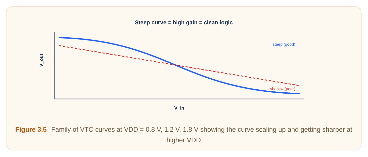
Gain is the steepness of the curve in the middle. It is the size of the output change divided by the input change. A steep curve has high gain. A gentle curve has low gain. High gain is what we want. A small, noisy input still produces a fully committed output. The gate "snaps" to a clean rail. It does not linger in the gray zone.
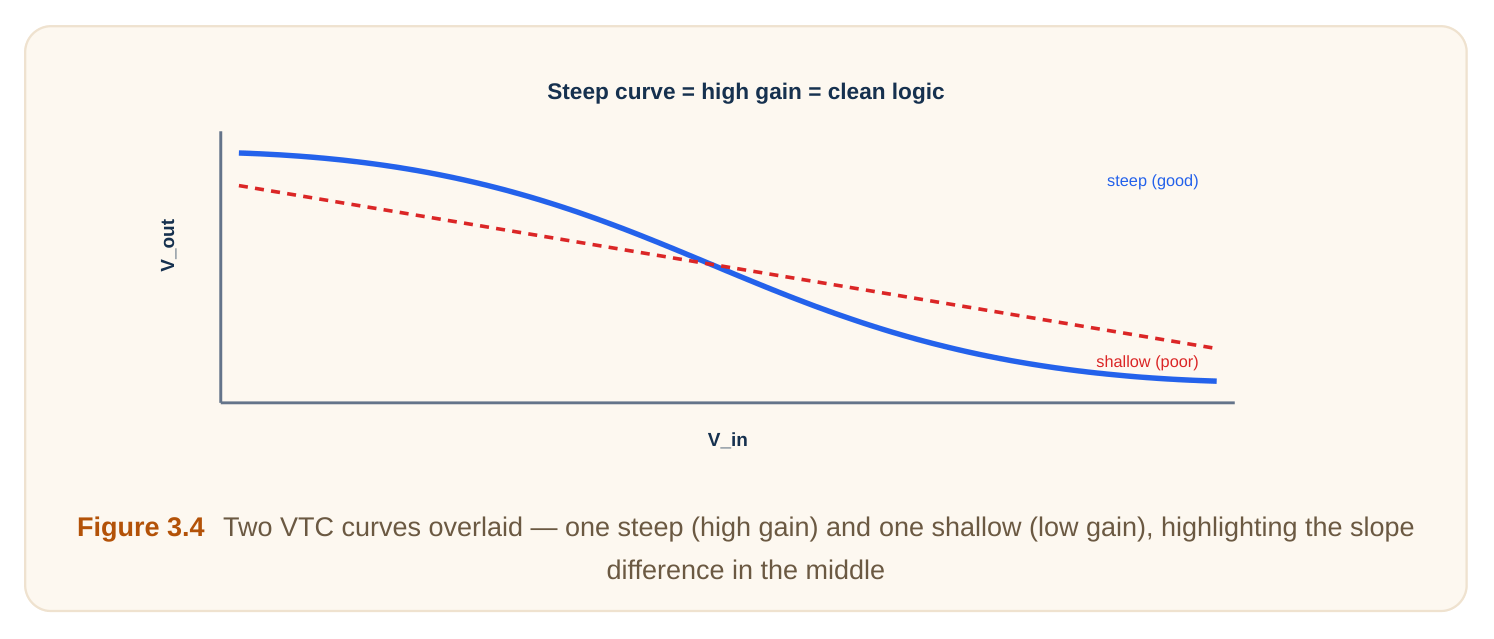
The slope at VM is the peak gain. A perfect digital gate would have infinite gain. Then the curve would be a vertical line. Real gates fall short, but higher is always better. Gain also sets the spacing of VIH and VIL. Remember, those points sit where the slope is −1. A steeper curve squeezes VIH and VIL closer together. That shrinks the gray zone. It widens both noise margins. So steepness and noise margin are linked. A steep curve gives clean logic and strong noise immunity at once. This is the core reason CMOS inverters make good building blocks.
Effect of Supply Voltage
The supply voltage VDD scales the whole curve. A higher VDD stretches the curve taller and wider. The output swings over a bigger range. A bigger swing usually means bigger absolute noise margins. More volts of buffer protect the signal. But higher VDD also burns more power. Power rises with the square of the supply. So designers balance noise safety against energy cost. When VDD drops very low, near the threshold voltages, the curve loses its sharp shape. Both transistors struggle to turn fully on. Gain falls. Noise margins shrink. This sets a floor on how low we can safely run.
Effect of the Beta Ratio
The beta ratio is the ratio of NMOS strength to PMOS strength. It bends the curve left or right. It does not change the height. It changes where the cliff sits. A strong NMOS pulls the cliff to the left. VM drops. The gate favors reading inputs as high. So NMH grows and NML shrinks. A strong PMOS pulls the cliff to the right. VM rises. The gate favors reading inputs as low. So NML grows and NMH shrinks.
TABLE 4: HOW THE BETA RATIO SHIFTS THE GATE
| Beta ratio condition | VM moves | NMH | NML |
|---|---|---|---|
| NMOS stronger | Down (left) | Larger | Smaller |
| Balanced | Centered | Balanced | Balanced |
| PMOS stronger | Up (right) | Smaller | Larger |
The lesson is clear. Balance the transistors to balance the margins. For most general logic, a centered VM is the safe default. Skew it only when you know one input edge needs extra protection.
Putting It Together
The inverter curve teaches three big ideas. A sharp middle gives clean logic. Full rail-to-rail output gives big noise margins. Balanced transistor strength centers the tipping point. These ideas repeat in every CMOS gate.
Interview Q&A
In region 3, both the NMOS and PMOS are in saturation. Both behave like current sources with high output resistance. A small input change shifts both currents strongly. The output then swings hard. This gives the steepest part, the highest gain, of the whole curve.
You balance the drive strength of the two transistors. NMOS carries more current than PMOS of the same size, because electrons are faster than holes. So you widen the PMOS by roughly the mobility ratio. With equal strength, VM lands near half the supply. That centers the gate.
NMH = VOH − VIH = 1.2 − 0.8 = 0.4 V. NML = VIL − VOL = 0.4 − 0.1 = 0.3 V. The high margin is 0.4 V and the low margin is 0.3 V. They are close but not equal. The gate is slightly stronger at protecting highs.
High gain means the output commits fully even when the input is noisy or weak. The gate snaps to a clean rail instead of resting in the gray zone. High gain also pushes VIH and VIL closer together. That widens both noise margins. So gain gives both clean logic and noise immunity.
The switching threshold VM moves up toward the supply. The cliff shifts right. The gate becomes biased to read inputs as low. This raises the low noise margin but lowers the high noise margin. The margins become unequal, which weakens the gate against high-side noise.
Key Takeaways
- The DC transfer curve plots output against input. It has five regions and a steep middle.
- Region 3, with both transistors in saturation, gives the steep cliff and highest gain.
- The switching threshold VM is where output equals input. It marks the tipping point.
- VM depends on the beta ratio. Widen the PMOS by the mobility ratio to center VM.
- VOH, VOL, VIH, and VIL define valid logic levels. CMOS swings rail to rail.
- NMH = VOH − VIH and NML = VIL − VOL measure noise tolerance. Bigger is safer.
- High gain shrinks the gray zone, widening both margins and giving clean logic.
- Higher supply gives bigger margins but costs more power. Very low supply weakens the curve.
- A balanced beta ratio gives balanced, robust noise margins on both sides.
Comments
Leave a Reply