 ChipBuddy
← Home
ChipBuddy
← Home
Quick Reference & Interview Q&A
How to Use This Chapter
This is the wrap-up. It pulls the whole book into quick tables and a question bank. Use it the night before an interview. Read the tables to refresh. Then practice the questions out loud. Aim to answer each in about 30 seconds, with the reasoning, not just the term.
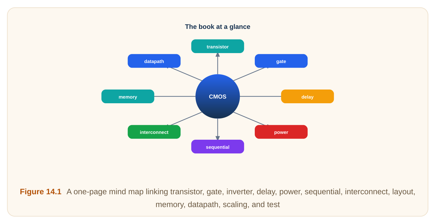
One-Page Concept Map
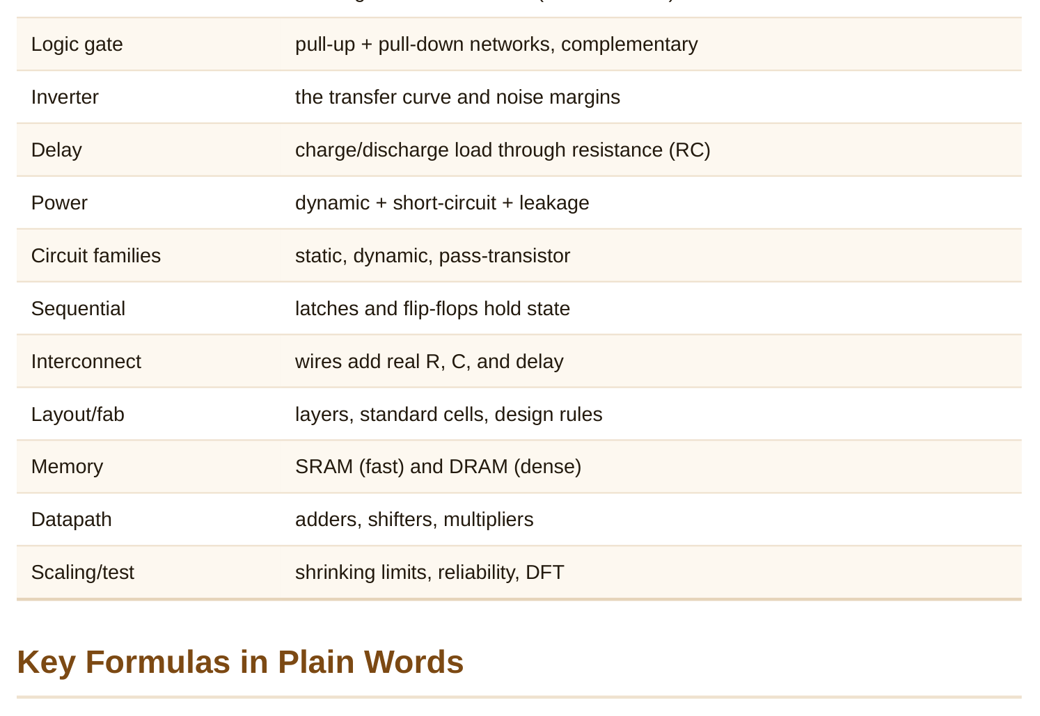
The book builds up in layers. Each layer rests on the one before.
| Layer | Core idea |
|---|---|
| Transistor | a voltage-controlled switch (NMOS/PMOS) |
You do not need heavy math for interviews. But know these relationships.
| Quantity | Plain relationship |
|---|---|
| Gate delay | grows with resistance × load capacitance (R·C) |
| Dynamic power | grows with activity × capacitance × voltage² × frequency |
| Max clock speed | 1 / (clock-to-Q + logic delay + setup) |
| Hold safety | clock-to-Q + short-path delay > hold + skew |
| Wire delay | grows with the square of length (without repeaters) |
| Shift left by N | multiply by 2 to the power N |
Quick Comparison Tables
Storage elements
| Latch | Flip-flop | |
|---|---|---|
| Trigger | clock level | clock edge |
| Transparent | yes | no |
| Build | one latch | master-slave (two) |
Memory
| SRAM | DRAM | |
|---|---|---|
| Cell | 6 transistors | 1 transistor + 1 cap |
| Refresh | no | yes |
| Use | cache | main memory |
Power components
| Type | Cause | Lever |
|---|---|---|
| Dynamic | switching load cap | lower V, clock gating |
| Short-circuit | both nets on briefly | sharp edges |
| Leakage | off-state current | multi-Vt, power gating |
Interview Q&A — Devices and Gates
In steady state only one network conducts, so static current is near zero. Outputs swing fully rail to rail, giving strong noise margins. Low static power plus robust logic levels made it the default.
toward the high rail, so it cannot pull a node fully high. A PMOS turns off as its source falls toward ground, so it cannot pull fully low. That is why CMOS pairs them: NMOS pulls down, PMOS pulls up.
when inputs are high, and the pull-up connects to the supply when inputs are low. So a rising input tends to lower the output. Building a non-inverting function needs an extra inversion stage.
NMOS. If they are balanced, the threshold sits near mid-supply. Making the PMOS stronger shifts it higher; a stronger NMOS shifts it lower. Sizing centers the threshold for symmetric noise margins.
Interview Q&A — Delay and Power
transistor's resistance. So delay scales with R times C. A bigger transistor lowers R (faster) but adds input capacitance (a load on the previous stage). That trade-off drives sizing.
stage handles a manageable ratio of load to drive. This staged approach beats one giant driver, which would overload the previous stage. The idea is to keep each stage's "effort" reasonable.
dynamic power scales with voltage squared. Halving the voltage cuts dynamic power to about a quarter. The cost is slower gates, so it trades speed for power. Clock gating (cutting activity) is the next big lever.
dropped. Both raise off-state current, which flows all the time. Leakage grew from negligible to a large share of total power. Multi-Vt cells and power gating exist to fight it.
Interview Q&A — Sequential and Memory
edge. Hold is how long it must stay steady after. Both exist because the storage element needs real time to sample and lock a value. Violating either gives a wrong or unstable capture.
and 1 after data changes too near the edge. It resolves in a random time, never with zero failure chance. Synchronizers (extra flops in series) give it more time to settle, making failure very rare.
large — used for caches. DRAM uses one transistor and a capacitor, is tiny and dense, but slow and needs refresh because charge leaks — used for main memory.
only a little, so the read signal is tiny. A sense amplifier amplifies that small difference into a clean full logic level, quickly and reliably, which makes fast, correct reads possible.
Interview Q&A — Interconnect, Layout, Scaling, Test
add real delay. Long wires can dominate a path. Wire delay grows with the square of length unless you insert repeaters, which break it into shorter, faster segments.
polysilicon (the gate) crosses an active region. A standard cell is a pre-designed gate layout of fixed height that tiles into rows with shared power and ground rails, enabling automatic placement.
more density, speed, and lower power per function. It slowed because voltage stopped dropping (leakage floor), so power no longer scaled down — the voltage and power walls.
The tester loads a known pattern into every flop, runs one cycle, and shifts results out. This gives full control and observation of buried state, making manufacturing test practical.
function faults, but they give every path extra time, so they miss delay faults. At-speed testing enforces the real clock period and catches paths that work but are too slow.
Rapid-Fire Round
Does lowering voltage help dynamic power a little or a lot? A lot — it scales with voltage squared.
needs refresh? DRAM. Q22. What breaks a long wire's quadratic delay? Repeaters (buffers along the wire). Q23. What makes buried flops testable? Scan chains. Q24. Transmission gate fixes what problem? The weak-level pass of a single transistor. Q25. Most power-hungry net on a chip? The clock network.
Final Study Checklist
Before the interview, be sure you can:
- Draw and explain a CMOS inverter and a NAND gate.
- State setup, hold, and clock-to-Q, and compute max frequency.
- Explain the three power components and the top lever for each.
- Compare SRAM and DRAM and explain refresh.
- Explain why wires now limit speed and how repeaters help.
- Explain scan and why DFT is needed.
- Explain what scaling gives and why it slowed.
Key Takeaways
- The book builds in layers: transistor → gate → inverter → delay/power → sequential → interconnect → layout → memory → datapath → scaling/test.
- Know the plain-word relationships: delay ∝ R·C, dynamic power ∝ activity·C·V²·f, max speed = 1/(clk-to-Q + logic + setup).
- Be fluent on the big comparisons: latch vs flop, SRAM vs DRAM, the three power components.
- Practice answers in ~30 seconds with reasoning; interviewers want the why, not just the definition.
- Use the final checklist to confirm you can explain and sketch each core idea on demand.
Comments
Leave a Reply