 ChipBuddy
← Home
ChipBuddy
← Home
Switching Speed & the RC Delay Model
Why a Gate Is Not Instant
A logic gate does not flip its output the moment its input changes. There is always a small wait. This wait matters a lot in fast chips. The reason is simple. Every gate output drives some load capacitance (an electrical "bucket" that stores charge). To change the output voltage, the gate must fill or empty that bucket. The gate fills or empties the bucket through its transistors. A transistor that is "on" behaves like a resistor (something that limits current flow). Current can only move so fast through a resistor. So the delay comes from two things working together. There is resistance that slows the flow. There is capacitance that needs charge moved into or out of it. Think of pouring water. A wide hose (low resistance) fills a cup fast. A narrow straw (high resistance) fills the same cup slowly. A bigger cup (more capacitance) always takes longer.
Drive strength = hose width
wide hose: fast fill narrow straw: slow fill
Figure 4.1 Water analogy — wide hose vs narrow straw filling a cup (capacitor)
The Simple RC Switch Model
We model a transistor switch as a plain resistor. We call its value R (the on-resistance of the transistor). When the transistor turns on, charge flows through this R. We model the load as a single capacitor. We call its value C (the total capacitance the gate must drive). This C sits between the output node and ground. When the output rises, the PMOS (the pull-up transistor) connects C to the supply. When the output falls, the NMOS (the pull-down transistor) connects C to ground. Inverter as a switch (R) charging a load (C) VDD R (on-transistor) C (load) delay ≈R × C
Figure 4.2 Inverter redrawn as a switch (R) connected to a load capacitor (C)
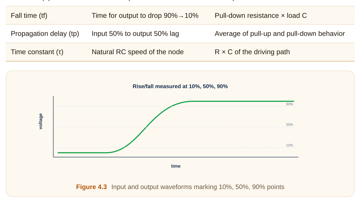
The voltage on a capacitor does not jump. It moves smoothly along a curve. The math of an RC circuit gives an exponential curve (a fast start that slowly levels off). The key result is this. The natural time constant of the circuit is R times C. We write this product as τ (the Greek letter "tau"). A larger τ means a slower gate. So propagation delay is roughly proportional to R × C. Cut either R or C in half, and the delay roughly halves too. This is the single most useful idea in this chapter. Speed is an RC problem. Almost every speed trick reduces R, reduces C, or both.
Rise Time, Fall Time, and Propagation Delay
Three timing terms appear in every interview. Let us define each one plainly.
Rise time is how long the output takes to go up. We usually measure it from 10% to 90% of the full swing. It is set by the pull-up path. Fall time is how long the output takes to go down. We also measure it from 90% down to 10%. It is set by the pull-down path. Propagation delay is the lag from input change to output change. We measure it at the 50% points of each signal. It is the number designers care about most.
| Term | Plain meaning | What sets it |
|---|---|---|
| Rise time (tr) | Time for output to climb 10%→90% | Pull-up resistance × load C |
Now, why does rise often differ from fall? It comes down to the two transistor types. The NMOS pulls the output low. It uses electrons, which move easily. So NMOS gives a low R and a quick fall. The PMOS pulls the output high. It uses holes, which move more slowly. Holes have lower mobility (a measure of how easily charge carriers move). For the same physical size, a PMOS has roughly two to three times the resistance of an NMOS. So a PMOS is the "weaker" transistor. A weaker pull-up means a slower rise. The output crawls up while it snaps down. This makes timing lopsided. The fix is sizing. We make the PMOS wider than the NMOS. A common ratio is making the PMOS about twice as wide. This balances rise and fall.
Where Load Capacitance Comes From
The load C is not one thing. It is the sum of several pieces. Knowing the pieces helps you cut them. The first source is fanout (the gates your output feeds). Each gate input has a gate capacitance. The more gates you drive, the more C you carry. The second source is wire capacitance. The metal wire from your output to the next gate stores charge. Long wires add a lot of C. The third source is self capacitance, also called parasitic capacitance. Your own transistors have drain capacitance at the output. This load is there even with nothing attached.
| Capacitance source | What it is | How to reduce it |
|---|---|---|
| Fanout cap | Input cap of gates you drive | Drive fewer gates; use buffers |
| Wire cap | Cap of the connecting metal | Shorter wires; smart placement |
| Self / parasitic cap | Your own drain diffusion cap | Smaller output transistors |
The total load is the sum of all three. The driving gate must charge this whole total. So a node with long wires and high fanout is slow.
Drive Strength and Sizing
Drive strength means how hard a gate can push charge. A strong gate has low R. It charges a load fast. We raise drive strength by making transistors wider. A wider transistor is like a wider hose. More current flows, so R drops. Doubling the width roughly halves the resistance. So a 2× gate is about twice as fast at driving the same load. This sounds like a free win. But there is a cost. A wider transistor has a bigger gate. A bigger gate has more input capacitance. So your faster gate is now a heavier load for whatever drives it. You made your own delay smaller. You made the previous stage's delay larger.
| Sizing trade-off | Make transistor wider | Make transistor narrower |
|---|---|---|
| Output resistance R | Goes down (faster) | Goes up (slower) |
| Input capacitance | Goes up (heavier load) | Goes down (lighter load) |
| Area used | More | Less |
| Power | More | Less |
This is the central tension of sizing. You cannot make everything wide. The cost just moves upstream. Good design balances the chain. Drive strength = hose width
wide hose: fast fill narrow straw: slow fill
Figure 4.4 Wider transistor — lower R but larger gate cap shown as a bigger input bucket
Fanout, Effort, and Buffer Chains
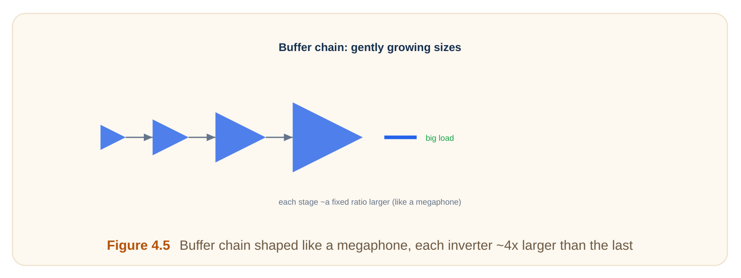
Now we reach a beautiful idea. How do you drive a huge load fast? Like a big output pad or a long bus. Your first instinct might be one giant gate. But a giant gate has a giant input. Whatever feeds it is now slow. You just moved the problem. A second instinct is one small gate. But a small gate has high R. It charges the huge load very slowly. Also bad. The smart answer is a chain of buffers (inverters that grow in size). Each stage is a bit bigger than the last. The signal ramps up in strength gently. The key concept is effort. Effort is how much bigger the load is than your own input. We can think of it as the ratio of output load to input size.
| Term | Plain meaning |
|---|---|
| Fanout | How many gates one output drives |
| Electrical effort | Load capacitance ÷ your own input capacitance |
| Stage effort | The work one gate does to drive the next |
| Logical effort | How a gate's own structure adds difficulty |
There is a sweet spot for stage effort. If each stage is too big a jump, that stage is slow. If each jump is tiny, you need too many stages. The classic result is that the best jump per stage is about 3 to 4. Often people use a factor of e (about 2.7) in theory. In practice, around 3 to 4 works well. So to drive a load 64× your size, you do not jump in one step. You grow by about 4× each stage. Four stages give 4×4×4×4 = 256, which is plenty.
The picture is a megaphone. A small voice feeds a small horn, then a bigger horn. Each stage amplifies smoothly. The big load gets driven fast.
What Increases Delay, and Why
It helps to gather every speed enemy in one place. An interviewer may ask you to list them. Each one maps back to R or C. A weak driver raises R. A small transistor has a narrow channel. Less current flows, so charging is slow. A heavy load raises C. High fanout, long wires, and big drains all pile on. The bucket gets bigger. A low supply voltage also hurts. Less voltage means less drive current. The transistor turns on less firmly, so R effectively rises. A high temperature slows things too. Heat lowers carrier mobility. Lower mobility means higher resistance and slower switching. A slow input edge adds delay as well. If the input ramps up lazily, the gate spends time half-on. The output cannot move cleanly until the input commits.
| What increases delay | Effect on the model | Simple reason |
|---|---|---|
| Weak / small driver | R goes up | Narrow channel, less current |
| High fanout | C goes up | Many input caps to charge |
| Long wires | C goes up | More metal stores charge |
| Low supply voltage | Effective R up | Weaker drive current |
| High temperature | R goes up | Mobility drops with heat |
| Slow input slope | tp goes up | Gate lingers half-on |
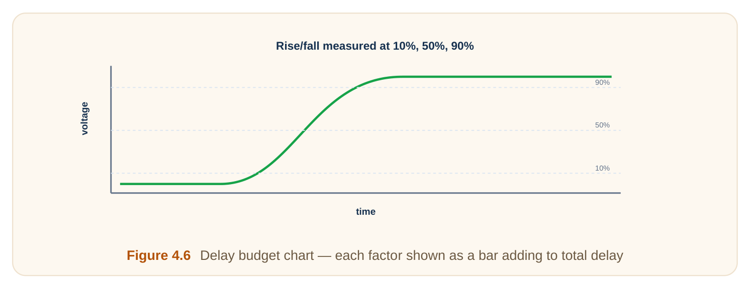
Notice the pattern. Almost every entry traces to R, C, or both. That is why the RC model is so powerful. It captures the whole story with two numbers.
Reading Delay as a Quick Estimate
In an interview you rarely run a simulator. You estimate in your head. The RC model makes this easy. The rule of thumb is delay equals about 0.7 times R times C. The 0.7 is the 50% factor we met earlier. To compare two designs, you can skip the 0.7 and just compare R × C products. The faster design has the smaller product.
Worked Example 1: Delay from R and C
Let us estimate a delay. Suppose a gate has on-resistance R = 5 kilohms. It drives a load C = 20 femtofarads. First find the time constant τ. We multiply R by C. So τ = 5,000 ohms × 20 × 10⁻¹⁵ farads. That gives τ = 100 × 10⁻¹² seconds. So τ = 100 picoseconds (a picosecond is one trillionth of a second). Propagation delay is measured at the 50% point. For an RC curve, the 50% point happens at about 0.69 × τ. This factor comes from the natural log of 2. So tp ≈ 0.69 × 100 ps. That gives tp ≈ 69 picoseconds. That is our delay estimate. Now suppose the wire doubles the load to C = 40 fF. Then τ doubles to 200 ps. The delay roughly doubles to about 138 ps. This shows how wire cap hurts speed.
Worked Example 2: Sizing to Halve the Delay
Take the first gate again. It has R = 5 kΩ and drives C = 20 fF. Its delay was about 69 ps. We want to cut that in half. We will reduce R, since the load C is fixed by the next stages. To halve delay, we halve R. We need R = 2.5 kΩ.
Resistance drops as width grows. To halve R, we double the transistor width. So we make the gate 2× wider. The new delay driving the same 20 fF is about 35 ps. We hit our target. Speed doubled for this stage. But check the cost. The input capacitance also doubled. If the gate's old input cap was 4 fF, it is now 8 fF. So the stage before it now drives 8 fF instead of 4 fF. That earlier stage got slower. The system gain is smaller than it looks. Always check both sides.
Worked Example 3: Choosing Buffer Stages for a Big Load
Now drive a large load. Our final load is C = 1,600 fF. Our starting gate has input cap of 5 fF. First find the total electrical effort. We divide load by input. So effort = 1,600 ÷ 5 = 320. We want each stage to grow by about 4×. So we ask how many 4× jumps reach 320. We compute powers of 4. 4¹ = 4, 4² = 16, 4³ = 64, 4⁴ = 256, 4⁵ = 1,024. The value 320 sits between 4⁴ and 4⁵. So four or five stages is right. Let us pick the stage factor that gives exactly four stages. We take the fourth root of 320, which is about 4.23. So each inverter is about 4.23× the size of the one before it. Four stages in a chain. This drives the big load far faster than one giant gate. A rough delay check helps. Each stage has effort about 4.23. Per-stage delay scales with effort plus a small self-load term. Four modest stages beat one stage of effort 320 by a wide margin. Compare it to the one-gate approach. A single gate facing effort 320 would be painfully slow. Its delay scales with that whole 320. The four-stage chain pays only about 4.23 per stage. This is why output drivers always look like growing chains. Look at any chip pad driver. You will see a row of inverters, each bigger than the last. That shape is no accident.
A Note on Logical Effort
We used a factor of about 4 per stage. That came from electrical effort alone. Real gates add one more twist called logical effort. Logical effort measures how a gate's structure adds difficulty. An inverter is the easiest gate, so its logical effort is 1. We use it as the baseline. A NAND gate is a bit harder to drive than an inverter. A NOR gate is harder still. This is because their stacked transistors raise resistance.
| Gate type | Rough logical effort | Why |
|---|---|---|
| Inverter | 1 | Simplest structure, baseline |
| 2-input NAND | ~4/3 | NMOS in series, some extra R |
| 2-input NOR | ~5/3 | PMOS in series, weak devices stacked |
The full delay rule multiplies logical effort by electrical effort. We call this product the stage effort. The best chain keeps each stage effort near 4. So the buffer-chain idea still holds for any gate. You just fold in the gate's own logical effort. The plain intuition stays the same: grow gently, stage by stage.
Interview Q&A
onto or off the load capacitor. It does this through the transistor's on-resistance. An RC circuit settles on a timescale set by R × C. So bigger R or bigger C means a longer settling time and more delay.
uses holes. Holes have lower mobility than electrons, so a PMOS has higher resistance than an equalsize NMOS. Higher pull-up resistance gives a slower rise. We fix it by sizing the PMOS wider, often about twice the NMOS width.
There is fanout cap from the gate inputs you drive. There is wire cap from the connecting metal. There is self or parasitic cap from your own drain diffusion. The total of all three is what the gate must charge.
resistance but larger input capacitance. The bigger input becomes a heavier load for the previous stage. So you slow down the stage that drives you. The cost moves upstream rather than disappearing, so you must balance the whole chain.
resistance and charges slowly. One giant gate has a huge input that slows its driver. A chain that grows by about 4× per stage spreads the work. This gives the lowest total delay for driving a large load.
Key Takeaways
- A gate is not instant because it must charge or discharge a load capacitor through transistor resistance.
- The simple model treats the transistor as a resistor R and the load as a capacitor C; delay is roughly proportional to R × C.
- Rise time, fall time, and propagation delay describe output timing; delay is read at the 50% point, near 0.69 × τ.
- PMOS is weaker than NMOS because holes move slower, so rise can lag unless the PMOS is sized wider.
- Load capacitance comes from fanout, wires, and self parasitics; cutting any of these speeds the gate.
- Wider transistors lower R and add speed, but they raise input capacitance, so the cost shifts to the previous stage.
- To drive a big load fast, use a chain of buffers that grow by about 3 to 4× per stage.
Comments
Leave a Reply