 ChipBuddy
← Home
ChipBuddy
← Home
Packaging & Power Delivery
Why Packaging and Power Delivery Matter
A chip by itself is just a small piece of silicon. It cannot work until it is placed inside a package. A package is the protective shell that holds the silicon die (the raw chip cut from a wafer) and connects it to the outside world. The package gives the chip mechanical strength, removes heat, and routes electrical signals and power in and out. Power delivery is the job of getting clean, steady voltage to every transistor on the chip. This sounds simple, but it is one of the hardest problems in modern design. A large chip can draw tens of amperes of current. That current must travel from a board, through the package, into the die, and out to billions of transistors. Along the way, the voltage can sag, spike, and wobble. When power delivery is poor, the chip slows down or fails. Many high-performance designs are limited not by the transistors themselves, but by how well power can be delivered. This chapter explains packages, the power distribution network, and the noise problems that come with delivering power.
There are two main ways to connect the die to the package. The first is wire-bond. The second is flipchip. Each connects the die's pads (small metal contacts on the chip surface) to the package in a different way. In a wire-bond package, the die sits face-up. Thin metal wires, often gold or copper, are welded from the die's edge pads to the package leads. Each wire carries one signal or one power connection. Wirebond is cheap and mature. But the wires are long and thin, so they add inductance (a property that resists fast changes in current) and resistance. The connections are also limited to the edge of the die. In a flip-chip package, the die is turned upside down, or "flipped." Small balls of solder, called bumps, are placed across the whole bottom face of the die. The die is then pressed onto the package so every bump lands on a matching pad. Because bumps cover the entire die area, not just the edge, flip-chip allows far more connections. The connections are also short, so they add much less inductance.
The table below compares the two approaches.
| Feature | Wire-Bond | Flip-Chip |
|---|---|---|
| Die orientation | Face-up | Face-down |
| Connection type | Thin metal wires | Solder bumps |
| Connection location | Die edge only | Whole die area |
| Number of connections | Lower (hundreds) | Higher (thousands) |
| Connection inductance | Higher | Lower |
| Cost | Lower | Higher |
| Best for | Low pin-count, low cost | High pin-count, high power |
For high-power, high-speed chips, flip-chip is almost always chosen. The many short bump connections let designers spread power across the whole die.
Bumps and the Power Path
A bump is a tiny ball of solder, often around 80 to 150 micrometers wide in a coarse design, or much smaller in advanced designs. Bumps are arranged in a grid across the die. Some bumps carry signals. Many bumps carry power and ground. Why use many power bumps? Because current must spread evenly. If only a few bumps carried power, current would crowd into a small area and cause heating and voltage loss. By using hundreds of power and ground bumps, current enters the die at many points at once. This keeps the path short from the bump to the nearest transistor. The full power path has several stages. Power starts at a voltage regulator on the board. It travels through board copper, into the package, through the package planes and vias (vertical metal connections between layers), up through the bumps, and finally into the on-chip metal grid. Each stage adds some resistance and some inductance.
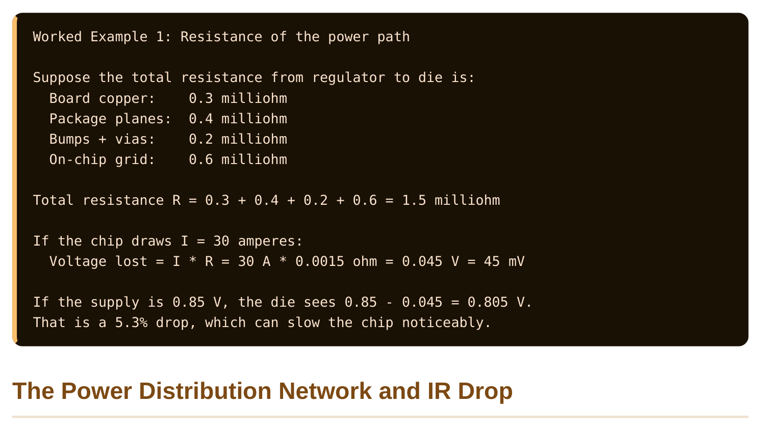
The power distribution network, or PDN, is the full set of metal that carries power and ground across the chip. On-chip, the PDN is built as a grid of wide metal lines on the upper metal layers. These lines form rings and stripes that blanket the design. Lower layers tap off this grid to feed individual standard cells (the small pre-built logic blocks like gates and flip-flops). IR drop is the voltage lost across the resistance of the PDN. The name comes from Ohm's law: voltage equals current (I) times resistance (R). When current flows through the resistive metal, some voltage is dropped before it reaches the transistor. The transistor then runs at a lower voltage than the supply, which makes it switch more slowly. There are two kinds of IR drop. Static IR drop is the steady voltage loss from average current. Dynamic IR drop is the brief, larger loss that happens when many gates switch at the same instant. Dynamic drop is usually worse and harder to fix.
The table below shows how IR drop affects timing.
| Supply at cell | Relative delay | Notes |
|---|---|---|
| 0.85 V (nominal) | 1.00x | Target speed |
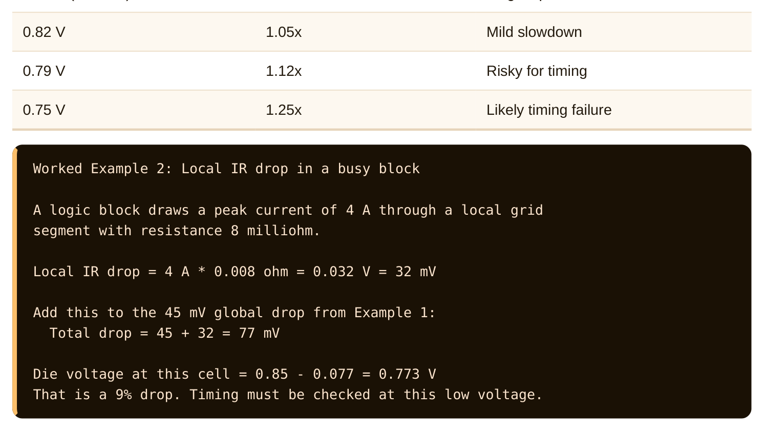
To fight IR drop, designers widen the grid metal, add more power bumps, and place high-current blocks near strong supply points. They also run sign-off checks that map IR drop across the whole die.
Decoupling Capacitors and Ldi/dt Noise
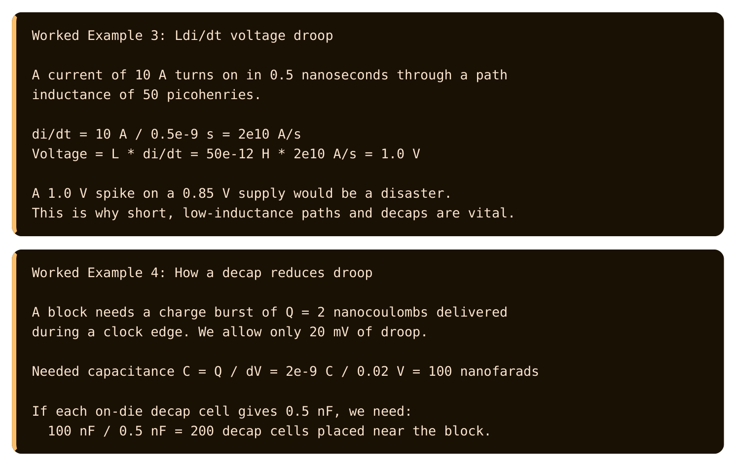
Current demand on a chip is not steady. When a clock edge arrives, millions of gates switch at once and pull a sudden burst of current. The PDN has inductance, and inductance resists fast current changes. This causes a voltage droop right when the chip needs power most. The noise from inductance is called Ldi/dt noise. The formula is voltage equals inductance (L) times the rate of change of current (di/dt). A fast current change across even a small inductance makes a real voltage spike. This noise is also called simultaneous switching noise, because it is worst when many outputs switch together. Decoupling capacitors fight this noise. A decoupling capacitor, often called a "decap," is a small capacitor placed close to the load. It stores charge and releases it instantly when the gates demand a burst. It acts like a tiny local battery that fills the gap before the far-away regulator can respond.
Decaps come at several levels. On-die decaps are fastest but small. Package decaps are larger and a bit slower. Board decaps are largest and slowest. Together they cover a wide range of frequencies.
| Decap location | Size | Speed of response | Frequency range covered |
|---|---|---|---|
| On-die | Smallest | Fastest | Very high frequency |
| Package | Medium | Medium | Mid frequency |
| Board | Largest | Slowest | Low frequency |
Why Power Delivery Limits Performance
Faster chips switch more transistors per second, so they draw more current and sharper current bursts. Both effects make power delivery harder. At some point, the chip cannot run faster because the supply cannot stay clean. There are three main limits. First, IR drop lowers the local voltage and slows the gates. Second, Ldi/dt noise causes droops that can corrupt logic or break timing. Third, heat from high current limits how much power the package can safely carry. Designers trade these limits against each other. Lowering the supply voltage cuts power and heat, but it shrinks the margin against droop. Raising the voltage speeds the gates, but it adds heat and current. Good power delivery widens the safe window in which the chip can run fast.
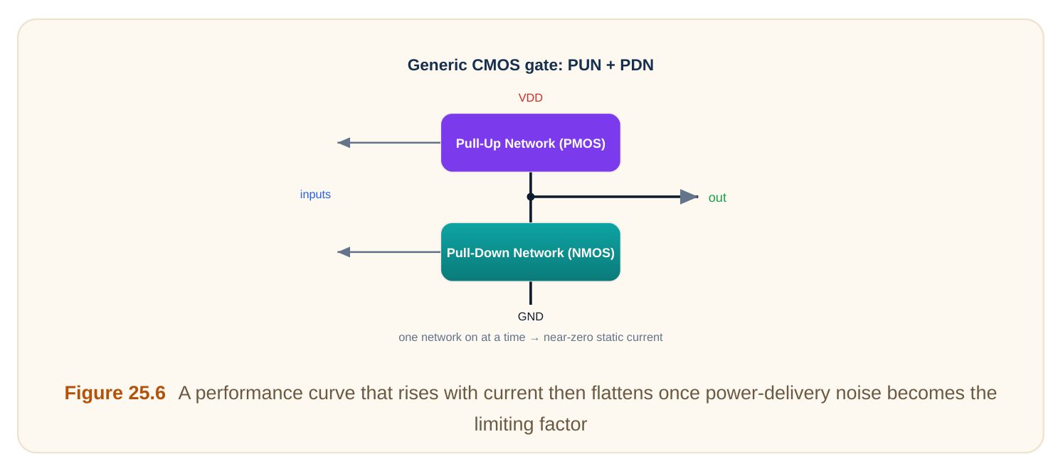
This is why teams spend so much effort on bumps, grids, and decaps. The transistors may be capable of more, but the chip can only go as fast as power delivery allows.
Interview Q&A
face-up and uses thin wires from edge pads to the package. Flip-chip turns the die face-down and uses solder bumps across the whole die area. Flip-chip allows many more connections and lower inductance, so it suits high-power, high-speed chips. Wire-bond is cheaper and fine for lower pin counts.
power grid, equal to current times resistance. It matters because the transistor then runs at a lower voltage than the supply, which makes it switch more slowly and can cause timing failures.
from average current. Dynamic IR drop is the larger, brief loss that happens when many gates switch at the same instant. Dynamic drop is usually worse and harder to control.
current. When many gates switch together, current changes quickly, and the inductance creates a voltage spike equal to inductance times the rate of current change.
charge. When gates demand a sudden current burst, the decap releases charge instantly, filling the gap before the distant regulator can respond. This reduces voltage droop.
sharper bursts. This worsens IR drop, Ldi/dt noise, and heat. At some point the supply cannot stay clean enough, so the chip cannot run faster even if the transistors could.
Key Takeaways
- Flip-chip uses bumps across the whole die for many short, low-inductance connections, while wire-bond uses edge wires and is cheaper but more limited.
- IR drop is voltage lost across grid resistance and directly slows the gates that see the lower voltage.
- Ldi/dt noise comes from inductance resisting fast current changes and is worst during simultaneous switching.
- Decoupling capacitors act as local charge reservoirs and are layered across die, package, and board to cover many frequencies.
- Power delivery is often the true limit on performance, since clean voltage cannot be maintained beyond a certain current and switching speed.
Comments
Leave a Reply