 ChipBuddy
← Home
ChipBuddy
← Home
Building CMOS Logic Gates
This chapter shows how real logic gates are built. We use CMOS (Complementary Metal-OxideSemiconductor) transistors. By the end, you can build any gate from a logic expression.
The Core CMOS Idea
Every CMOS gate has two halves. One half pulls the output up. The other half pulls the output down. The top half is the pull-up network (PUN). It connects the output to the supply voltage. We call the supply VDD (the positive power rail). The PUN uses only PMOS transistors (transistors that turn on with a low gate voltage). The bottom half is the pull-down network (PDN). It connects the output to ground. Ground is the zerovolt rail, often called GND. The PDN uses only NMOS transistors (transistors that turn on with a high gate voltage). These two halves are complementary. When one half conducts, the other half blocks. They are never both on in steady state. Think of two doors on a tank. The top door fills it; the bottom door drains it. Only one door opens at a time.
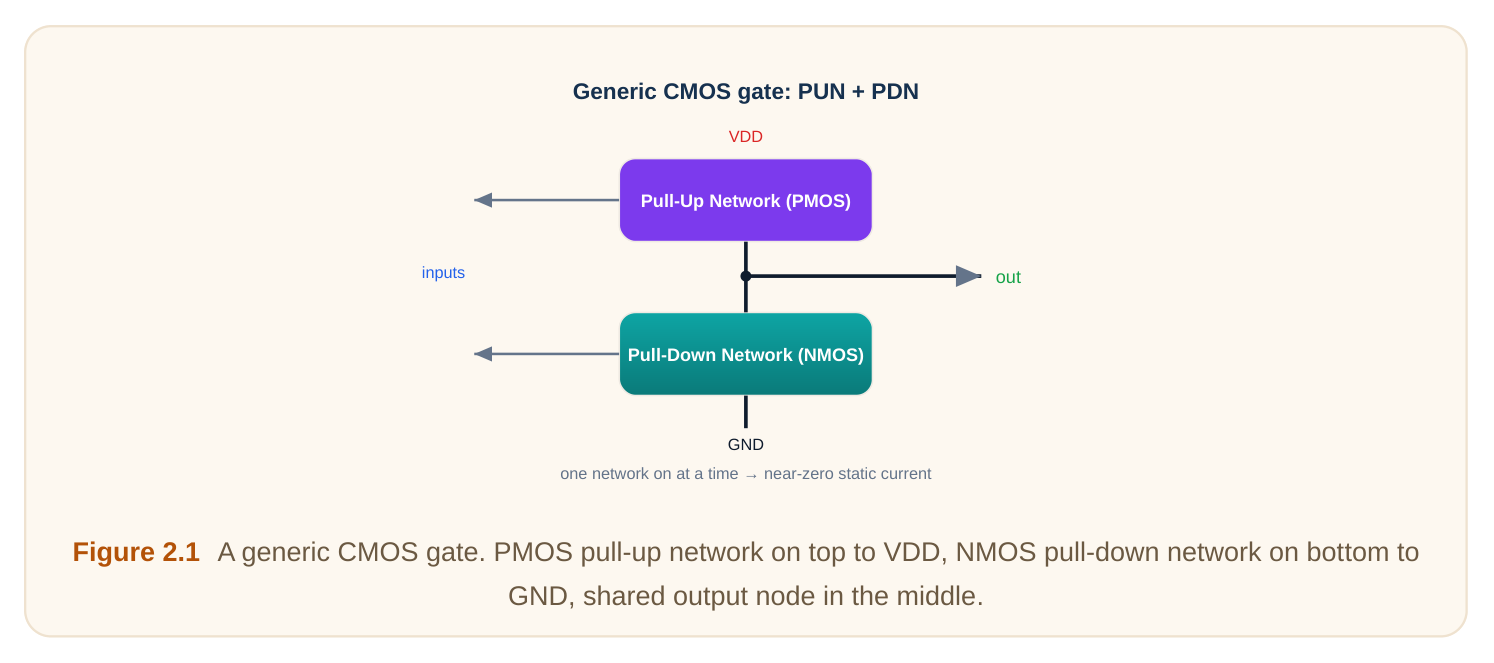
A PMOS turns on when its gate sees a low signal. An NMOS turns on when its gate sees a high signal. The same input drives both. So one transistor opens while its partner closes. This automatic swap is the heart of CMOS. Why use two different transistor types? Each type has a job it does well. NMOS transistors pass a strong low. They pull the output cleanly down to ground. PMOS transistors pass a strong high. They pull the output cleanly up to VDD. So we use NMOS to pull down and PMOS to pull up. Each transistor plays to its strength. This split is not optional. An NMOS is poor at passing a high. A PMOS is poor at passing a low. By giving each its natural job, CMOS gets clean output levels.
Why Static Current Is Near Zero
In steady state, only one network conducts. There is no direct path from VDD to ground. No path means no current flows straight through. Power equals voltage times current. With near-zero current, static power is near zero. "Static" means the input is not changing. This is why CMOS won the chip world. It sips power while idle. Current only flows briefly when inputs switch. During a switch, both networks may conduct for a moment. That brief overlap draws a small "short-circuit" current. But while resting, the gate is nearly silent. Compare this to older logic styles. Some older gates used a resistor as the pull-up. A resistor always leaks current when the output is low. That wastes power all the time. CMOS removed the resistor and used a transistor instead. The transistor turns fully off, so the leak stops. There is still a tiny leakage current in real chips. Transistors are not perfect switches. A small current sneaks through even when off. This is called leakage. But it is still far smaller than a constant resistor path.
Why Outputs Swing Fully
A CMOS output reaches a clean high or a clean low. We call this full-swing output. When the PUN conducts, it ties the output straight to VDD. The output rises all the way to VDD. When the PDN conducts, it ties the output straight to ground. The output falls all the way to zero. No weak resistor sits in the path to steal voltage. So a logic "1" is a strong VDD. A logic "0" is a strong ground. Strong levels resist noise. This makes the next gate read the value clearly.
The Inverter: The Simplest Gate
The inverter (a NOT gate) is the smallest CMOS gate. It has one PMOS and one NMOS. Both share the same input. Feed in a low. The PMOS turns on; the NMOS turns off. The output is pulled to VDD, so it reads high. Feed in a high. The PMOS turns off; the NMOS turns on. The output is pulled to ground, so it reads low. The output is always the opposite of the input. That is inversion.
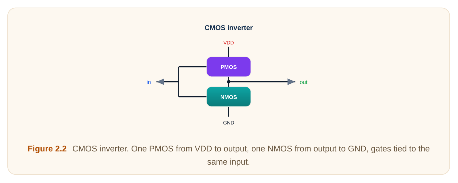
This pattern repeats in every gate. PMOS on top, NMOS on bottom, complementary action. Larger gates just add more transistors to each network.
NAND and NOR: Series and Parallel
Bigger gates combine transistors in series or parallel. Series means transistors stacked one above the other. Both must be on to conduct. Parallel means transistors side by side. Either one on lets it conduct. A 2-input NAND gate works like this. The pull-down network has two NMOS in series. The pull-up network has two PMOS in parallel. The output goes low only when both inputs are high. Both series NMOS must turn on to pull down. If either input is low, one PMOS turns on and pulls up.
A 2-input NOR gate is the mirror. The pull-down network has two NMOS in parallel. The pull-up network has two PMOS in series. The output goes low if either input is high. Any single NMOS can pull it down. The output goes high only when both inputs are low.
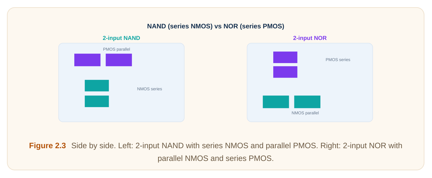
Table 2.1: NAND vs NOR Structure
| Feature | 2-input NAND | 2-input NOR |
|---|---|---|
| Pull-down (NMOS) | Series | Parallel |
| Pull-up (PMOS) | Parallel | Series |
| Output low when | Both inputs high | Any input high |
| Output high when | Any input low | Both inputs low |
| Transistor count | 4 | 4 |
| Slow path | NMOS stack of 2 | PMOS stack of 2 |
The Series-Parallel Duality Rule
There is a simple pattern linking the two networks. It is called duality. In the pull-down network, an AND of inputs means transistors in series. An OR of inputs means transistors in parallel. The pull-up network does the exact opposite. Series in one network becomes parallel in the other. Here is the rule in plain words. Series in the PDN maps to parallel in the PUN. Parallel in the PDN maps to series in the PUN. The two networks are mirror images.
Table 2.2: Pull-Up / Pull-Down Construction Rules
| Logic relation between inputs | Pull-down (NMOS) | Pull-up (PMOS) |
|---|---|---|
| Inputs ANDed | Series | Parallel |
| Inputs ORed | Parallel | Series |
| Single input | One transistor | One transistor |
This duality keeps the two halves complementary. When the PDN finds a path, the PUN cannot. When the PUN finds a path, the PDN cannot. So the rule guarantees the no-overlap behavior. Here is an easy way to remember it. Picture the pull-down network first. Build it directly from the logic you want. Then flip every series link to parallel. Flip every parallel link to series. That flipped copy is your pull-up network. The shapes are mirror images of each other. This trick always works for static CMOS gates. You never guess the pull-up. You build one half, then mirror it.
Worked Example 1: Derive a 2-Input NAND
Let us build a 2-input NAND step by step. Call the inputs A and B. Call the output Y. The NAND function is Y = NOT(A AND B). The output is low only when A AND B are both high. Step 1: Build the pull-down. The output goes low when A AND B. "AND" means series. So place two NMOS in series. The top NMOS has gate A. The bottom NMOS has gate B. Both must be on to pull Y down. Step 2: Build the pull-up by duality. Series in the PDN becomes parallel in the PUN. So place two PMOS in parallel. One PMOS has gate A. The other has gate B. Either can pull Y up. Step 3: Check the truth table.
Table 2.3: 2-Input NAND Operation
| 0 | 0 | off | both on | 1 |
|---|---|---|---|---|
| 0 | 1 | off | A's PMOS on | 1 |
| 1 | 0 | off | B's PMOS on | 1 |
| 1 | 1 | both on | off | 0 |
The output is low only on the last row. That matches NAND exactly. The total transistor count is four.
Building Complex Gates: AOI and OAI
Real chips rarely use only NAND and NOR. They use compound gates. These pack a small logic expression into one gate.
Two common types exist. AOI stands for AND-OR-Invert. It computes ANDs, ORs them, then inverts. OAI stands for OR-AND-Invert. It computes ORs, ANDs them, then inverts. Compound gates save transistors. They also save delay. One compound gate can replace several simple gates. This is a big reason CMOS designers love them. To build one, read the expression and apply the rules. ANDed terms go in series in the PDN. ORed terms go in parallel in the PDN. Then build the PUN by duality.
Worked Example 2: Build an AOI Gate
Let us build an AOI gate for this function. Y = NOT( (A AND B) OR C ). Read the inside first. We AND A with B. We OR that result with C. Then we invert everything. The invert is automatic in CMOS. Step 1: Build the pull-down. The expression inside is (A AND B) OR C. "A AND B" means series, so stack NMOS A over NMOS B. "OR C" means parallel, so place NMOS C beside that stack. Now the PDN pulls Y low when (A AND B) OR C is true. Step 2: Build the pull-up by duality. Series becomes parallel; parallel becomes series. The A-B series pair becomes a PMOS A parallel PMOS B group. The OR with C becomes a series connection. So put PMOS C in series with the parallel PMOS A and PMOS B pair. Step 3: Count and check. The PDN has three NMOS. The PUN has three PMOS. Total is six transistors. Let us spot-check two cases. Set A=1, B=1, C=0. Inside = (1 AND 1) OR 0 = 1. Output = NOT 1 = 0. In the circuit, the A-B NMOS stack conducts and pulls Y low. Correct. Set A=0, B=0, C=0. Inside = 0. Output = NOT 0 = 1. No NMOS path exists. The PMOS network conducts and pulls Y high. Correct.
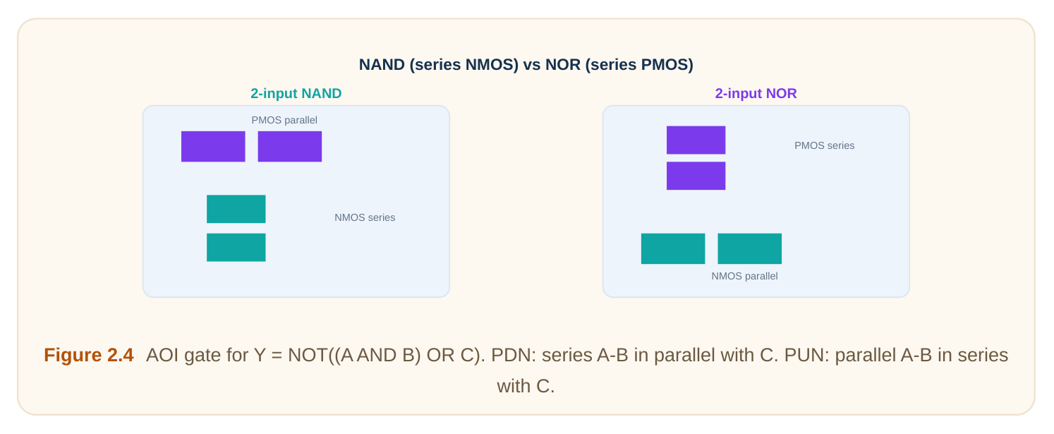
This single gate replaces an AND, an OR, and an inverter. That would be many more transistors built separately.
Let us count the savings. Built from simple gates, this needs an AND, an OR, and a NOT. A CMOS AND is six transistors. A CMOS OR is six. A NOT is two. That is fourteen transistors and three stages of delay. The single AOI gate does it in six transistors and one stage. That is a huge win in both area and speed. This is why designers think in AOI and OAI forms. They rewrite logic to match these gates. A skilled designer reads an expression and sees the gate at once.
Why CMOS Gates Are Naturally Inverting
Notice a pattern. Every basic CMOS gate inverts. NAND, NOR, and AOI all end with "invert." The reason is physical. When inputs are high, the NMOS network conducts and pulls the output low. High inputs give a low output. That is inversion built into the structure. NMOS transistors pull down well. PMOS transistors pull up well. The natural arrangement gives a low output for active inputs. So pure CMOS gates cannot directly make AND or OR. They make NAND, NOR, AOI, and OAI.
Making Non-Inverting Functions
Sometimes you truly need AND or OR. The output must follow, not invert. The fix is simple. Add an inverter at the output. A NAND followed by an inverter gives AND. A NOR followed by an inverter gives OR. This costs two extra transistors. It also adds one stage of delay. So designers avoid it when they can. Often they redesign the logic to absorb the inversions. A chain of NAND gates can compute almost anything. Bubbles (inversions) cancel in pairs along a path.
Transistor Count and Speed
Every input drives one NMOS and one PMOS. So a gate needs two transistors per input. A 2-input gate has four. A 3-input gate has six.
Table 2.4: Gate to Transistor Count
| Gate | Inputs | Transistors | Inverting? |
|---|---|---|---|
| Inverter (NOT) | 1 | 2 | Yes |
| 2-input NAND | 2 | 4 | Yes |
| 2-input NOR | 2 | 4 | Yes |
| 3-input NAND | 3 | 6 | Yes |
| AOI (A·B + C) | 3 | 6 | Yes |
| 2-input AND | 2 | 6 | No (NAND + inverter) |
Series stacking hurts speed. Stacked transistors act like resistors in a line. More transistors in series means more total resistance. Higher resistance means slower charging of the output. So a tall stack switches slowly. This is why NAND is often preferred over NOR. NAND stacks NMOS in series. NOR stacks PMOS in series. PMOS carry current more weakly than NMOS of the same size. A PMOS stack is slower than an NMOS stack. So NOR's slow path is worse. Designers favor NAND-based logic for speed. To keep stacks fast, designers limit stack height. Three or four in series is a common ceiling. Beyond that, they split logic across more gates. They also make stacked transistors wider. Wider transistors carry more current and lower resistance. Think of a stack like a row of straws joined end to end. One straw is easy to suck through. Five straws in a line make it hard. The path resistance adds up. Water, or here current, moves slowly. So a tall stack drains the output slowly and the gate is slow.
A Quick Build Recipe
Here is the full method in five short steps. Use it for any static CMOS gate. First, write the function with the inversion on the outside. Second, look at the inside expression. Third, build the pull-down: ANDs become series, ORs become parallel. Fourth, mirror the pull-down to get the pull-up. Fifth, check a few input cases against the truth table. Follow these steps and you cannot go wrong. The method works for NAND, NOR, AOI, OAI, and beyond. It is the single most useful skill in this chapter.
Interview Q&A
network conducts. The pull-up and pull-down are complementary. So there is no direct path from VDD to ground. No through-path means near-zero static current. Power is voltage times current, so static power is tiny.
images. ANDed inputs are series in the pull-down and parallel in the pull-up. ORed inputs are parallel in the pull-down and series in the pull-up. Building one network gives the other by swapping series and parallel.
high. "Either" means OR, and OR means parallel. So place two NMOS in parallel. One gate is A; the other is B. Either transistor on pulls the output low.
on the NMOS network and pull the output low. So active inputs give a low output, which is inversion. To make a non-inverting AND, build a NAND and add an inverter at its output. That costs two extra transistors and one stage of delay.
NMOS in series. PMOS conduct more weakly than equal-size NMOS. A series PMOS stack has higher resistance, so it charges the output slowly. NAND's worst path uses faster NMOS, so NAND switches quicker.
Key Takeaways
- Every CMOS gate has a PMOS pull-up to VDD and an NMOS pull-down to ground.
- The two networks are complementary. Only one conducts at a time.
- This gives near-zero static current and full-swing, noise-resistant outputs.
- The inverter is the simplest gate: one PMOS, one NMOS.
- NAND uses series NMOS and parallel PMOS; NOR is the reverse.
- Duality rule: series in one network is parallel in the other.
- Read any expression to build the pull-down, then mirror it for the pull-up.
- AOI and OAI compound gates pack logic into one gate and save transistors.
- CMOS gates are naturally inverting; add an inverter for AND or OR.
- Each input needs two transistors. Tall series stacks slow the gate down.
- NAND is usually faster than NOR because NMOS stacks beat PMOS stacks.
Comments
Leave a Reply