 ChipBuddy
← Home
ChipBuddy
← Home
Scaling, Reliability & Variation
Why Smaller Got Better — and Then Harder
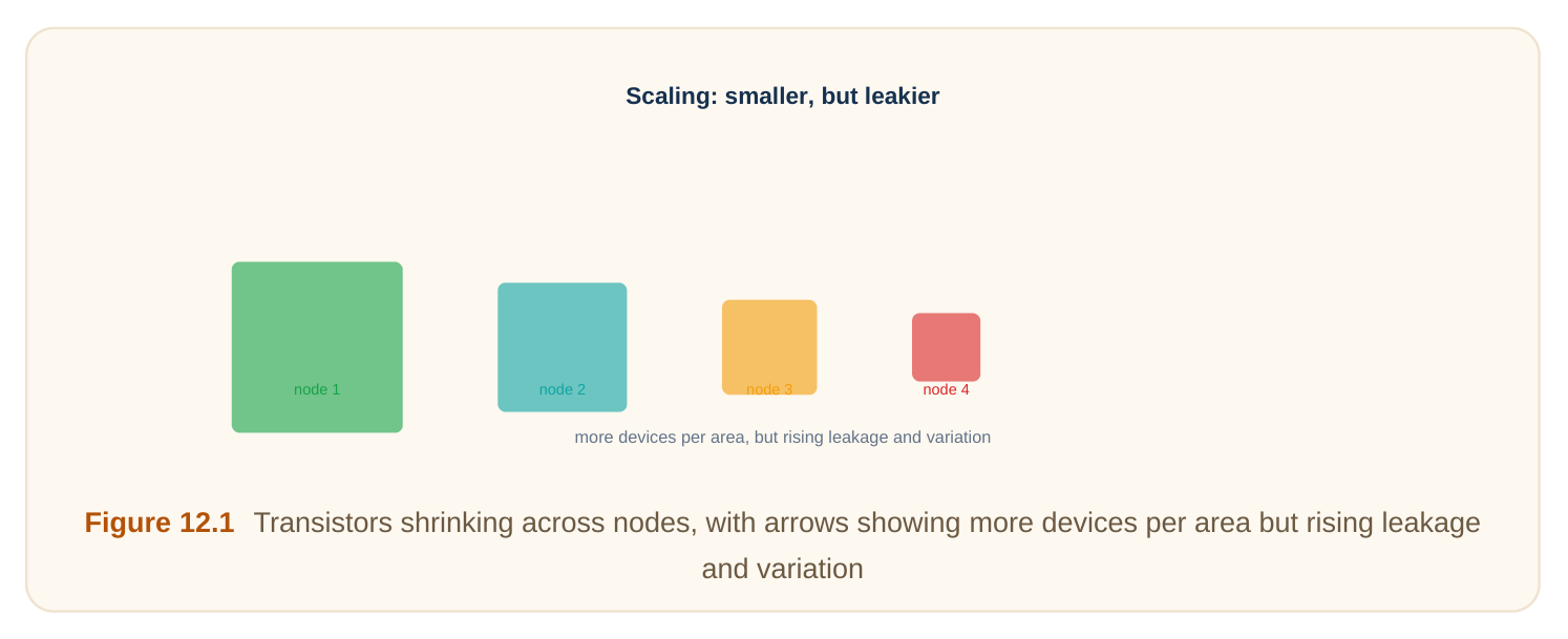
For decades, chips improved by making transistors smaller. Smaller meant faster, cheaper, and lower power per function. This shrinking is called scaling. But scaling eventually ran into hard physical walls. This chapter explains what scaling buys, why it slowed, and the reliability and variation problems that come with tiny devices.
Classic Scaling: the Good Years
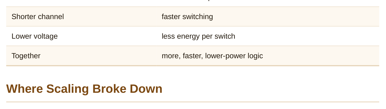
The simple idea: shrink every dimension by the same factor. Make the transistor narrower, shorter, and thinner. Lower the voltage too. When all of this scales together, good things happen.
- More transistors fit in the same area. Density rises sharply.
- Each transistor switches faster. Speed improves.
- Each switch uses less energy. Power per function drops. This balanced shrink is called ideal (or Dennard) scaling. For many generations it worked beautifully. Every new node gave more, faster, cooler logic. Scaling effect Result Smaller dimensions more devices per area
The clean story ended. A few walls appeared.
- Voltage stopped scaling well. The threshold voltage cannot drop much without leakage exploding. So supply voltage flattened out.
- Leakage rose. Thin gates and low thresholds leak current even when off. Static power became a big share of total power.
- The power wall. You can fit more transistors than you can safely power on at once. Heat limits how much can switch. Some logic must stay dark. This is sometimes called "dark silicon".
- Wires did not improve like transistors. Gates got faster, but wires did not. Interconnect delay became a bigger share. So modern scaling gives more transistors. But not the easy speed and power wins of the past. Wall Cause Effect Voltage wall threshold can't drop supply voltage flattens Leakage wall thin gates, low Vt static power grows Power/thermal wall heat limit not all logic can switch Wire wall wires scale poorly interconnect dominates delay
Worked example — power does not shrink for free
Say a node shrink doubles the transistor count in the same area. In the old days, voltage also dropped enough that total power stayed flat. Now voltage barely drops. So doubling the transistors can nearly double the power. The chip cannot run all of them at full speed at once. That is the power wall in one example.
New Tricks to Keep Scaling
When simple shrinking stalled, designers changed the device and the methods.
- Better transistor shapes: wrapping the gate around the channel on more sides gives better control and less leakage. This keeps small devices usable.
- Strain and new materials: small changes to the silicon and gate improve speed and reduce leakage.
- Multi-Vt cells: mix fast (leaky) and slow (low-leakage) transistors. Use fast ones only where needed.
- Power gating and clock gating: shut off idle blocks and idle clocks to fight leakage and dynamic power.
- Parallelism over frequency: add more cores instead of pushing one core faster, since frequency hit the power wall. The theme: when the device physics gets harder, design technique does more of the work.
Reliability: Chips Wear Out
A new chip is not the end of the story. Chips age. Several effects slowly shift behavior over years.
- Electromigration (EM): high current slowly erodes metal wires. Over time a wire can thin and open. Wide power and clock wires fight this.
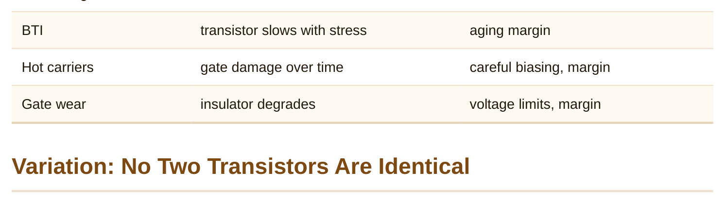
- Bias-temperature instability (BTI): transistors get a bit slower with use, especially when hot and stressed. Threshold voltage drifts.
- Hot-carrier effects: energetic carriers damage the gate over time, also shifting behavior.
- Time-dependent gate wear: the thin gate insulator can degrade and eventually fail. Because of aging, sign-off adds margin. The chip must still meet timing at end-of-life, not just on day one.
| Reliability effect | Plain meaning | Defense |
|---|---|---|
| Electromigration | metal erodes under current | wider wires, current limits |
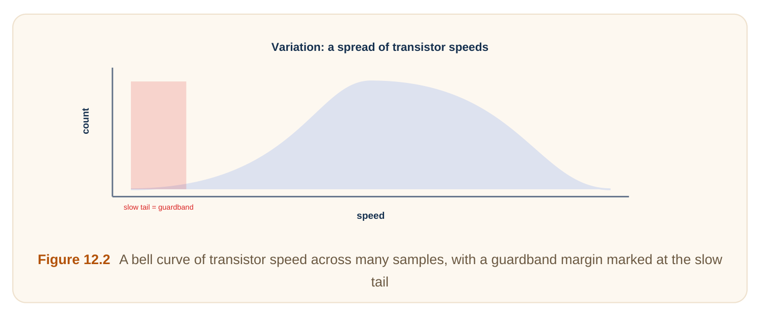
Two transistors drawn the same are never truly identical. Tiny manufacturing differences make them slightly faster or slower. This is variation. At small sizes, it gets worse, because a few atoms matter. There are two flavors.
- Systematic variation: predictable patterns. For example, density or position on the wafer. You can model and correct some of it.
- Random variation: unpredictable, cell to cell. For example, random dopant placement. You handle it with statistical margin. Variation forces designers to add guardband (extra safety margin). Too little margin risks failures. Too much margin wastes speed and power. Modern sign-off uses statistical methods to spend margin wisely.
Worked example — variation eats margin
Suppose a path is designed to run at 1.00 ns. Variation might make a slow sample of the chip 8% slower. So you must plan for about 1.08 ns. That extra 0.08 ns is pure margin. It buys yield (the fraction of chips that work). But it costs speed. Statistical timing tries to keep this margin as small as safely possible.
Putting It Together
Scaling gave the industry decades of gains. Now the easy gains are gone. More transistors still arrive each node. But speed, power, reliability, and variation all push back. Modern design wins by combining better devices with smart techniques: gating, multi-Vt, parallelism, and statistical margining. The interview message: know both what scaling gives and what it now costs.
Interview Q&A
voltage together gave more density, more speed, and less power per function. It stopped mainly because voltage could no longer drop much (the threshold floor), so leakage rose and total power no longer scaled down — the voltage and power walls.
powered at once, because heat limits total switching. So part of the chip must stay idle ("dark") at any moment. You can integrate more logic than you can run simultaneously at full speed.
metal under high current — handled with wider power/clock wires and current limits. BTI slowly slows transistors under stress — handled by adding aging margin so the chip still meets timing at end-of-life. (Hot carriers and gate wear are similar.)
follows predictable patterns (density, wafer position) and can be partly modeled and corrected. Random variation is unpredictable cell to cell (e.g., random dopant placement) and is handled with statistical margin. Both make identical-drawn transistors behave differently.
core faster, designers added more cores (parallelism) and leaned on power gating, clock gating, and multi-Vt cells to manage power. Better device shapes (more gate control) and statistical margining keep tiny, leaky devices usable.
Key Takeaways
- Scaling (shrinking dimensions and voltage together) gave decades of more density, speed, and lower power per function.
- It slowed at the voltage, leakage, power, and wire walls; more transistors arrive, but not easy speed/power wins.
- Designers respond with better device shapes, multi-Vt, gating, and parallelism instead of pure frequency.
- Chips age: electromigration, BTI, hot carriers, and gate wear shift behavior, so sign-off adds end- of-life margin.
- Variation (systematic and random) makes identical transistors differ; it is managed with guardband and statistical timing.
Comments
Leave a Reply