 ChipBuddy
← Home
ChipBuddy
← Home
Nonvolatile & Emerging Memory
Nonvolatile and Emerging Memory
Most memory in a chip forgets everything when you turn off the power. That kind of memory is called volatile memory. Static RAM (SRAM, fast on-chip memory built from transistors) and dynamic RAM (DRAM, dense memory built from tiny capacitors) both lose their data without power. Nonvolatile memory (NVM, memory that keeps its data with the power off) does the opposite. It remembers. Your phone keeps photos and apps in nonvolatile memory. A washing machine keeps its settings there too. This chapter walks through the main nonvolatile families. We start with flash, the workhorse of the last few decades. Then we look at EEPROM, an older cousin. Then we meet the emerging types that may take over in some roles: MRAM, ReRAM, and PCM.
The Floating Gate and How Flash Stores a Bit
A normal MOS transistor (metal-oxide-semiconductor transistor, the basic switch in a chip) has one gate. Apply voltage to the gate and the device turns on. A flash cell adds a second gate buried inside the oxide. This buried gate is called the floating gate (a piece of conductor completely surrounded by insulator). It has no wire connected to it. Charge placed on it cannot easily leak away. That trapped charge is the stored bit.
When the floating gate holds electrons, it pushes back against the control gate. The cell now needs a higher voltage to turn on. We call that turn-on voltage the threshold voltage (the gate voltage at which the transistor starts to conduct). So the trick is simple. Empty floating gate means low threshold, which we read as one logic value. Charged floating gate means high threshold, which we read as the other value.
To put electrons onto the floating gate we use high voltage. Two physical effects do the work. One is hot-carrier injection (fast electrons jumping through the thin oxide). The other is Fowler-Nordheim tunneling (electrons quantum-tunneling through a very thin oxide under a strong field). To remove electrons we reverse the field and tunnel them back out. That erase step is what gives flash its name, because early parts erased a whole block in a quick flash.
NOR Flash Versus NAND Flash
Flash comes in two layouts. The names come from the logic gates the cell arrangement resembles. NOR flash connects each cell so its drain (the terminal that current flows into) touches a shared bit line directly. Every cell can be reached on its own. This gives fast random reads. You can fetch any single word quickly. That is why NOR flash often stores code that the processor runs directly. NAND flash strings many cells in series, one after another, like beads on a string. This packs cells very tightly, so NAND is cheaper per bit. But you cannot read one cell alone. You read whole pages. NAND is the choice for bulk storage like memory cards and solid-state drives. The table below sums up the trade-off.
| Feature | NOR flash | NAND flash |
|---|---|---|
| Cell layout | Parallel, direct access | Series string |
| Density | Lower | Higher |
| Random read speed | Fast | Slow |
| Write/erase speed | Slow | Fast |
| Cost per bit | High | Low |
| Typical use | Code storage | Mass data storage |
Modern NAND also stacks cells vertically in many layers to pack even more bits into the same chip area. A flat design wastes area, while a tall stack reuses the footprint many times over.
Engineers also store more than one bit per cell. A cell that holds one bit uses two charge levels. A cell that holds two bits uses four charge levels. More levels mean more bits but also less margin between levels, so the cell wears out faster and reads slower.
| Cell type | Bits per cell | Charge levels | Relative endurance |
|---|---|---|---|
| Single-level | 1 | 2 | Highest |
| Multi-level | 2 | 4 | Medium |
| Triple-level | 3 | 8 | Low |
| Quad-level | 4 | 16 | Lowest |
Wear, Endurance, and Retention
Every erase pushes electrons hard through the thin oxide. Each trip damages the oxide a little. Over many cycles the oxide traps stray charge and the cell stops working cleanly. This slow damage is called wear. Endurance is the number of erase cycles a cell survives before it fails. A high-quality single-level cell might handle a hundred thousand cycles. A quad-level cell might handle only a few thousand. Retention is how long the cell keeps its data without power. A fresh cell may hold data for ten years. A worn cell leaks faster and holds it for less.
Worked Example 1: Endurance budget
A drive uses cells rated for 3,000 erase cycles.
The drive holds 512 GB.
The user writes 40 GB per day.
Naive cycles per day = 40 GB / 512 GB = 0.078 erase cycles per day
Days to wear out one cell evenly = 3,000 / 0.078 = 38,400 days
38,400 days / 365 = about 105 years
Lesson: if writes spread evenly, the drive lasts far
longer than the user will ever need.
The catch is that writes do not spread evenly on their own. One hot file would hammer the same cells. To fix this, controllers use wear leveling (spreading writes across all cells so they age together). The controller keeps a count for each block and steers new writes toward the least-used blocks.
Before flash, the common rewritable nonvolatile memory was EEPROM (electrically erasable programmable read-only memory). EEPROM also uses a floating gate. The key difference is granularity.
EEPROM lets you erase and rewrite one byte at a time. That is convenient for small settings, like a serial number or a calibration value. But supporting per-byte erase needs extra transistors per cell. That makes EEPROM bulky and expensive for large sizes. Flash gave up per-byte erase. It erases in large blocks instead. Giving up that flexibility let designers shrink the cell, and the cost per bit dropped sharply. So flash won the bulk storage market while EEPROM survives in tiny configuration roles.
| Property | EEPROM | Flash |
|---|---|---|
| Erase unit | One byte | Large block |
Flash has limits. Its writes are slow, its endurance is shrinking as cells get smaller, and it needs high voltage to write. Researchers have built new memory types to fix these problems. Three stand out. MRAM (magnetoresistive RAM) stores a bit as the direction of a tiny magnet. A small stack called a magnetic tunnel junction has two magnetic layers. When their magnetizations point the same way, resistance is low. When they point opposite ways, resistance is high. We read the bit by measuring resistance. Because magnets keep their direction with no power, MRAM is nonvolatile. It is fast and has very high endurance, almost like SRAM that remembers. ReRAM (resistive RAM) stores a bit by forming or breaking a tiny conductive path inside an insulating film. Apply one voltage and a thin filament of atoms bridges the film, giving low resistance. Apply the opposite voltage and the filament breaks, giving high resistance. ReRAM cells are small and simple, which makes dense arrays possible.
PCM (phase-change memory) stores a bit in the physical state of a special material. Heat the material and cool it fast, and it freezes into a disordered glassy state with high resistance. Heat it gently and let it settle, and it becomes an ordered crystal with low resistance. The two states are stable, so the bit stays put.
Worked Example 3: Reading a resistance-based cell
A ReRAM cell has two states:
Low-resistance state = 10 kilohms
High-resistance state = 1 megohm
Read voltage = 0.2 V
Low-state current = 0.2 V / 10,000 ohm = 20 microamps
High-state current = 0.2 V / 1,000,000 ohm = 0.2 microamps
Ratio of currents = 20 / 0.2 = 100 times
A 100x current gap is easy for a sense amplifier to tell apart.
These types share a big advantage. They read and write by resistance or magnetism, not by trapped charge forced through fragile oxide. That tends to mean faster writes, lower write voltage, and much higher endurance.
| Type | Stores bit as | Strength | Weakness |
|---|---|---|---|
| MRAM | Magnet direction | Fast, huge endurance | Lower density, cost |
| ReRAM | Conductive filament | Simple, dense | Cell-to-cell variation |
| PCM | Crystal vs glass | Good density, stable | High write energy |
The Memory Hierarchy
No single memory is best at everything. So systems stack several kinds in a hierarchy (a layered arrangement from small-fast to large-slow). Fast memory sits near the processor. Slow, cheap, dense memory sits farther away.
Worked Example 4: Picking memory for a smartwatch
Need: store the running program for instant access
-> use a small NOR flash, fast random read
Need: store user data and apps, large and cheap
-> use NAND flash
Need: scratch space the program works in, very fast
-> use SRAM and DRAM (volatile)
Need: a calibration constant set once at the factory
-> use a tiny EEPROM
Each role gets the memory that fits it best.
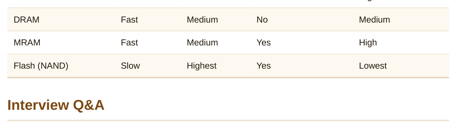
The emerging types aim for a sweet spot between fast volatile memory and slow flash. A memory that is nearly as fast as DRAM but keeps data with the power off would let a device wake up instantly and use almost no standby power.
| Memory | Speed | Density | Nonvolatile? | Cost per bit |
|---|---|---|---|---|
| SRAM | Fastest | Lowest | No | Highest |
negative charge. They repel the field from the control gate. So you must apply a higher gate voltage to overcome that repulsion and turn the transistor on. The shifted turn-on point is exactly how the cell encodes a stored bit.
and removes the per-cell direct contact that NOR needs. Fewer contacts and tighter spacing pack many more cells into the same area. More bits per area means lower cost per bit, at the price of slow random reads.
damages the oxide and lets it trap stray charge. After enough cycles the cell can no longer separate its charge states cleanly. That oxide wear sets the cycle count the cell can survive.
into the same silicon, cutting cost per bit. The cost is smaller voltage margin between the many charge levels. That smaller margin means slower reads, lower endurance, and shorter retention.
through fragile oxide. MRAM stores a bit as the direction of a tiny magnet and reads it as resistance. No charge crosses an oxide, so MRAM writes faster, uses lower voltage, and lasts vastly more cycles.
which suits small settings like calibration values and serial numbers. Flash erases only large blocks, so updating one byte would be wasteful. For tiny config data, byte-level access still wins.
Key Takeaways
- A floating gate traps charge to shift the threshold voltage, and that shift is the stored bit in flash and EEPROM.
- NOR gives fast random reads for code, while NAND gives cheap dense storage for bulk
data.
- Endurance is limited by oxide wear during erase, and wear leveling spreads writes so the whole array ages together.
- Storing more bits per cell lowers cost but cuts endurance, speed, and retention because voltage margins shrink.
- Emerging memories (MRAM, ReRAM, PCM) store bits by resistance or magnetism, promising faster low-voltage writes and far higher endurance than flash.
Comments
Leave a Reply